What do you want the simulator to do when absolute maximum Vebo is exceeded? Permanently short emitter to collector? Permanently reduce beta to 20% of its previous value? Permanently install a 10 gigohm resistor between internal-emitter and external-emitter?
I was thinking that the ~Zener behavior should be modeled. Using a small BJT as a ~6V Zener is common and could be used on MOSFET gates. But there are other situations where behavior under overdrive conditions should be simulated. You need to know when Vebo and Vceo will be violated.
A thermal (failure) model would also be useful, but simply not ignoring over voltage behavior would be very useful.
A thermal (failure) model would also be useful, but simply not ignoring over voltage behavior would be very useful.
There's a 15V On Semi transistor model that did the opposite for me. The circuit showed really low distortion and when I checked voltages I saw this one exceeded VCEO, so I changed it out for an appropriate VCEO transistor and distortion went up considerably. I didn't find any discrepancies when using the model within its limits, only when exceeding VCEO. This one or one of the other versions of it, though I can't seem to find a model on their website now.
So put a 7V (or 4.7V; it was handy) Zener across it. (With single simple diode in series so it does not swamp the emitter junction.)the ~Zener behavior should be modeled
I hope I got the polarities right.

I was considering creating a sub circuit that wraps any BJT where the BJT model, Vebo and Vceo are parameters. I don't want to clutter up all my schematics with extra parts. I was hoping I could just edit the models, but I tried that, and it did nothing. Ideal would be a new "NPN" and "PNP" model.
Go ahead, you can put PRR's circuit in a subcircuit.
A couple of years ago I worked with the Mextram transistor model at work. It includes weak avalanching, at least between collector and emitter, but since we wanted to know what would happen if the transistor were momentarily driven into strong avalanching, we ended up making a subcircuit with some non-linear controlled sources after all.
A couple of years ago I worked with the Mextram transistor model at work. It includes weak avalanching, at least between collector and emitter, but since we wanted to know what would happen if the transistor were momentarily driven into strong avalanching, we ended up making a subcircuit with some non-linear controlled sources after all.
Great! Thank you sir! But I can't find a parameter name for the collector??? Where did you find Bvbe ? Vceo does not seem to do anything.You can edit the models: for example:
View attachment 1099888
Strange things also happen in reality for voltages approaching or exceeding the collector-emitter breakdown voltage with open base VCEO, which is usually well below the collector-base breakdown voltage VCBO. Due to impact ionization in the collector-base region, the current gain goes to infinity at VCEO and negative above it (base current flowing out of the base, if there is something connected to the base that it can flow into) and you get snap-back behaviour.
There is a snap effect in the sim:

In the real world, the effect is caused by the dependence of Vceo on beta. At low currents, beta falls due to leakage currents, meaning Vceo tends toward Vcbo, but as soon as current starts to flow, beta increases and starts the runaway process, and the snap action.
Older transistors had a strong snap-back effect, because of process imperfections, but contemporary types are practically devoid of it.
However in the simulation, the 2N3904 model does not include parameters like ISE; IKF is present but has no effect on the breakdown behaviour.
LTspice must have a default mechanism to cause the effect
Is there any dependence on Gmin? If roll-off of the current gain isn't included, a 1 pS conductance between base and emitter just might cause it to snap back anyway.
Does the result look different at lower frequencies? Maybe in your simulation, capacitive effects are playing a role somehow. For example, collector-base capacitance charging the base, but less in the first cycle than in the others.
Does the result look different at lower frequencies? Maybe in your simulation, capacitive effects are playing a role somehow. For example, collector-base capacitance charging the base, but less in the first cycle than in the others.
See
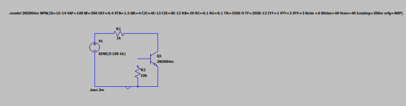
.model kt315g npn bf=250 is=100f vaf=60 ikf=50m xtb=1.5 br=2 rc=5 rb=200 rbm=20 irb=.3m cjc=15p vjc=.75 mjc=.33 fc=.5 cje=20p vje=.75 mje=.33 tr=250n tf=.5n itf=40m vtf=10 xtf=2 xti=3 eg=1.11 xcjc=0.15 ne=1.8 ise=20p nc=2 isc=600p BVbe=7 IBVbe=20u BVcbo=120 Vceo=35 Icrating=100m mfg=USSR
.model kt315g npn bf=250 is=100f vaf=60 ikf=50m xtb=1.5 br=2 rc=5 rb=200 rbm=20 irb=.3m cjc=15p vjc=.75 mjc=.33 fc=.5 cje=20p vje=.75 mje=.33 tr=250n tf=.5n itf=40m vtf=10 xtf=2 xti=3 eg=1.11 xcjc=0.15 ne=1.8 ise=20p nc=2 isc=600p BVbe=7 IBVbe=20u BVcbo=120 Vceo=35 Icrating=100m mfg=USSR
- Home
- Design & Build
- Software Tools
- BJT Vebo in spice?