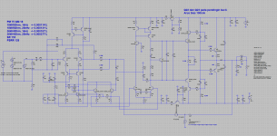
HEC amplifier topology created by Bob Cordell. I'm interested to make simulation using this topology.
It used 24VDC PSU and OITPC compensation that created by Dadod.
Output stage is simple using double emitter follower with driver bootstrapped. Using small transistor in driver,
make loop gain higher because their high hFE.
Any suggestion are welcome.
It used 24VDC PSU and OITPC compensation that created by Dadod.
Output stage is simple using double emitter follower with driver bootstrapped. Using small transistor in driver,
make loop gain higher because their high hFE.
Any suggestion are welcome.
Attachments


TP2.
R55 = 2R2 1W || 1uH.OK, Thank you.
Is R55 a jumper or low resister?
Isn't TP2 better for feedback points too?
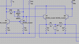
HEC is Q7 and Q8 in simulation, so LTP can be loaded with current mirror (Q5 and Q6).Pardon me if I'm dim late at night, but where is the HEC part of this circuit?

OK, I understand.
If you are targeting low distortion, the following can be obstacles.
Placing isolation inductors close to the OPS can exacerbate distortion under the magnetic field of those currents.
If the lead caps on both ends of the 2R2 resistor are iron, the coil wrapped around it can generate magnetic distortion.
I wish you good luck!
Thank you for the suggestion.If you are targeting low distortion, the following can be obstacles.
Placing isolation inductors close to the OPS can exacerbate distortion under the magnetic field of those currents.
If the lead caps on both ends of the 2R2 resistor are iron, the coil wrapped around it can generate magnetic distortion.
Yes, it targeting low distortion, high slew rate, and high PSRR.
It looks like the capacitor voltage in the bootstrap circuit near the output is getting clamped via Q22 base-collector and its base resistor to the rails when driven above certain level, and same for opposite lower side.
Also I don't see any HEC circuit incorporated around the output stage.
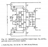
See Cordell's paper, figure 12, where Q22 and Q23 makes up part of the HEC circuit.
https://www.cordellaudio.com/papers/MOSFET_Power_Amp.pdf
edit: Hawksford HEC paper.
https://www.researchgate.net/publication/269099597_Distortion_Correction_in_Audio_Power_Amplifiers
Also I don't see any HEC circuit incorporated around the output stage.
See Cordell's paper, figure 12, where Q22 and Q23 makes up part of the HEC circuit.
https://www.cordellaudio.com/papers/MOSFET_Power_Amp.pdf
edit: Hawksford HEC paper.
https://www.researchgate.net/publication/269099597_Distortion_Correction_in_Audio_Power_Amplifiers
Attachments
Last edited:
I think HEC topology is about input and VAS stage. Edmond Stuart and Ovididu compare it (input and VAS stage) with other topology in their website. DR. Arto Kolinummi also mention it for input and VAS stage in his book (Audio Power Amplifier).It looks like the capacitor voltage in the bootstrap circuit near the output is getting clamped via Q22 base-collector and its base resistor to the rails when driven above certain level, and same for opposite lower side.
Also I don't see any HEC circuit incorporated around the output stage.
See Cordell's paper, figure 12, where Q22 and Q23 makes up part of the HEC circuit.
https://www.cordellaudio.com/papers/MOSFET_Power_Amp.pdf
How about adopting a 3D scheme to mitigate induction/interference - critical components to be placed vertically to make orthogonal fields when close to possible receivers?OK, I understand.
If you are targeting low distortion, the following can be obstacles.
Placing isolation inductors close to the OPS can exacerbate distortion under the magnetic field of those currents.
If the lead caps on both ends of the 2R2 resistor are iron, the coil wrapped around it can generate magnetic distortion.
I wish you good luck!
//
If HEC is Hwaksford Error Correction, maybe I should called it Bob Cordell's input stage amplifier.I think HEC topology is about input and VAS stage. Edmond Stuart and Ovididu compare it (input and VAS stage) with other topology in their website. DR. Arto Kolinummi also mention it for input and VAS stage in his book (Audio Power Amplifier).
I also made simulation of Output with Error Correction in this forum.
Maybe you can also comment in this thread: https://www.diyaudio.com/community/...as-current-of-output-error-correction.379517/
Ok I see now what you mean, that part is related to improvement of common mode rejection handling.HEC is Q7 and Q8 in simulation, so LTP can be loaded with current mirror (Q5 and Q6).
In Cordell's paper I linked to he writes on page 9 the following:
The input stage is loaded by current sources (Q6, Q7) to provide high open-loop gain at low frequencies, Emitter-followers Q8 and Q9 isolate the input stage from second-stage (predriver) loading effects and produce a combined common-mode feedback signal at the junction of R19 and R20 to properly bias Q6 and Q7.
This also provides additional common-mode rejection by reducing the common-mode impedance seen by the collectors of the input stage. Limiter diodes D2 and D3 prevent excessive signal swings at the collectors of Q4 and Q5 when the amplifier is clipping.
Operation of this circuit can be understood by looking at what would happen if the sum of the drain currents of Q1 and Q2 (i.e., the common-mode current) were to increase for some reason.
The collector currents of Q4 and Q5 would then exceed those of Q6 and Q7, respectively.
This would cause the base voltages of Q8 and Q9 to go in a negative direction, in turn causing the common-mode feedback signal at the junction of R19 and R20 to go in a negative direction. As a result, the collector currents of Q6 and Q7 would increase by the amount necessary to equal those of Q4 and Qs, thus restoring balance. Notice that this common-mode feedback loop acts to keep the voltage at the junction of R19 and R20 equal to the positive rail voltage less the combined voltage drop of an emitter resistor (R15 or R16 ) and a base-emitter junction (Q6 or Q7).
If the common-mode current supplied by Q3 were to increase the combined voltage drop of an emitter resistor (R15 by 0.1 mA, for example, this combined voltage drop would change by roughly 25 mV (primarily due to increased emitter resistor voltage drop). The common-mode voltage at the collectors of Q4 and Q5 would thus also change by 25 mV, implying a common-mode impedance at these nodes of 250 Ohm.
The effects of differential-mode current signals at the collectors of Q4 and Q5 sum to zero at the junction of R19 and R20.
Differential signals are thus unaffected by the common-mode feedback loop and see a high differential-mode impedance as a result.
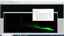
An interesting exercise to perform here could be to see how the amplifier circuit simulates and distortion figures and harmonic pattern changes by disabling the CMRR circuitry action by disconnecting (component annotation taken from post #1) Q5 and Q6 bases from the resistor divider (R8 and R10 I think, the picture has too poor resolution so I don't see very well, as with many other component numbers too) sitting in between Q7 and Q8 emitters (In Cordell's schematics attached just above that is: Q6-Q7, R19-R20 and Q8-Q9), and instead connect the bases to a fixed voltage source equaling the same voltage.
Last edited:
It won't work. DC Offset is -1.33V.An interesting exercise to perform here could be to see how the amplifier circuit simulates and distortion figures and harmonic pattern changes by disabling the CMRR circuitry action by disconnecting (component annotation taken from post #1) Q5 and Q6 bases from the resistor divider (R8 and R10 I think, the picture has too poor resolution so I don't see very well, as with many other component numbers too) sitting in between Q7 and Q8 emitters (In Cordell's schematics attached just above that is: Q6-Q7, R19-R20 and Q8-Q9), and instead connect the bases to a fixed voltage source equaling the same voltage.
Attachments
The current mirror won't work. And loop gain become very low.
- Home
- Amplifiers
- Solid State
- Simple HEC Amplifier 24VDC