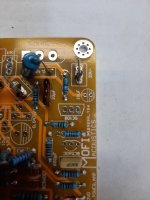
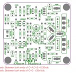
Can't figure out orientation of transistor BD139 to silkscreened board without E-C-B markings with only a trapezoid marking?? Can someone tell me which way to orient the transistor to solder? See attachment. Let me know if narrow part of silkscreen is front or back of transistor . I think I have E-C-B correctly marked. There is metal on rear of transistor.
Attachments

Can you post the schematic? There is not enough information to determine the right orientation.
If one of the pads is square, that would be pin #1.
If one of the pads is square, that would be pin #1.
Attached is picture of BD139 location. I know which transistor pin is 1-2-3 but not on the board for orientation to solder in. I would think that the trapezoid outline would be recognized by someone and say which hole is pin 1 or 3 to orient. Thanks for any help.
Attachments

That's not a standard footprint, so there's no way to tell. A square pin #1 would be typical.I would think that the trapezoid outline would be recognized by someone and say which hole is pin 1 or 3 to orient.
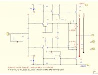
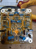
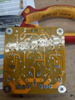
see attachment. What does this say? Bottom side trace to topside trace and this and that.............Hope the drawing attachment is correct. THe emitter of BC560 goes through electrolytic cap to get to -24 VDC. Can you name the inked location to pin 1 or 3 then we are in business. thanks for the help
Attachments

3, base is first from left and must go to emmiter of bc560
You must have made a mistake
You must have made a mistake
Thank-you sir for your help. Maybe I can keep the smoke from escaping this time..............3, base is first from left
Sorry but your schematic is USELESS as is.Attached is picture of BD139 location. I know which transistor pin is 1-2-3 but not on the board for orientation to solder in. I would think that the trapezoid outline would be recognized by someone and say which hole is pin 1 or 3 to orient. Thanks for any help.
PLEASE label ALL transistors as Q1, Q2 ... etc.
ALL resistors as R1 R2 ... etc.
Also ALL resistor values.
Otherwise we are like a Postman trying to deliver in a City with no street names and no house numbers.
Here is data sheet of BC560. I believe the EBC is correct in my drawing. The drawing is top view with lines from foil side. ThanksYou only switched collector and emitter of bc560
Attachments
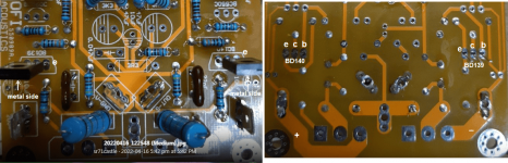
So with what you marked up. The transistor should be reversed so metal side points to your arrow? And now if I look closer you have the emitter point on the board marked with E. THank-you very much.Now we can see it 👍
Mona
The base of bd140 has to be directly connected with emmiter of bc560, no resistors between.
Simple as that.
What you draw in post #9 is misleading. Collector of bc560 is not dirrectly connected with base of bd140.
Are you purposely confusing us?
I am out. Good luck.
Simple as that.
What you draw in post #9 is misleading. Collector of bc560 is not dirrectly connected with base of bd140.
Are you purposely confusing us?
I am out. Good luck.
So as to your previous observation and doubts, was transistor BC560 labeled wrong? What is the answer? Instead without explanation a statement of "Are you purposely confusing us?. WOW.............Your statement is about BD140 NOT BD139 as what this was originally about. But still I appreciate your help and sorry if I made it confusing. That is why I am here and not a genius. Take care. OUTThe base of bd140 has to be directly connected with emmiter of bc560, no resistors between.
Simple as that.
What you draw in post #9 is misleading. Collector of bc560 is not dirrectly connected with base of bd140.
Are you purposely confusing us?
I am out. Good luck.
Attachments
- Home
- Design & Build
- Parts
- BD139 transistor board silkscreen minus E-C-B markings