Yes, the schematic is correct **, however in my case I didn't need (TTL) level conversion as my WaveIO has been modified to provide TTL level output. Whether or not you need conversion to TTL levels depends on your input - for example the following Toslink input board says it can output TTL levels http://www.twistedpearaudio.com/digital/torx.aspx, so you wouldn't need the TTL converter board if you used this.As fas as I understand, your solution converts a USB input to ST output; my understanding is described by the following schematics: see the attached diagram.
** the 1414TZ needs the complete Avago TX circuit built and +5V to function - it wasn't shown in the schematic, but I guess you know this.
Yes. If you just want a single input you could try a BNC or RCA terminated with 75R instead of the WaveIo board in your schematic. That should work. I say "should" because I've never used that TTL converter board, but think it may offer an easy OOB solution for you. As with any advice on the internet it's incumbent on the reader to satisfy themselves about what is said before spending money and time... 😉 The one thing I do know for sure is that the Avago circuit I posted works because I have built it.Your suggestion seems to replace the "WaveIo board" by another prebuilt board that would convert the [BNC or AES/EBU] signals to SPDIF signal, in order to feed the "Twisted Pear Audio" board. The rest of the diagram would remain unchanged.
The incoming signal should already be SPDIF (e.g. from CD player digital out). You probably don't need a prebuilt board unless you want toslink or switching for multiple inputs. It might pay just to go with a single input as described above for a POC before investing further.One of my Wadia inputs has been modified with an AVAGO receiver, and I am almost sure that it is an Avago 2416-TZ, probably matching with the 1414TZ that I have in my stock (the 2 other inputs are unchanged, so they should use a CTS ODL Series II).
If it is simpler to design a solution using the CTS ODL Series II, then I will by a CTS emitter.
Do I understand correctly ?
If yes, we still have to find a prebuilt board that would convert BNC to SPDIF: suggestions are welcome !
This isn't my area of expertise, but happy to help as I can. There should be heaps of threads on diyaudio about SPDIF input too..If we find such a board, then I could probably begin to build a solution, under your monitoring of course...🙂
Last edited:
I found a paper on spdif input for you - you can probably get away with the following for a BNC or RCA input (before the TTL board). The paper does a good job of explaining what R1 and C1 do on page 12. https://www.st.com/resource/en/appl...e-stm32f4-f7-h7-series-stmicroelectronics.pdf


There were 3 like this one originally, and one of them has been replaced by an AVAGO (see above for the reference), but the AVAGO does not improve the sound: the sound that I get out of the W9 is slightly better on the 2 remaining inputs with the original ST receivers.
You should ditch the AVAGO. Stick to the original CTS. The CTS ST transmitter will likely be the best match with your Wadia. There are some available to buy.
Heres the datasheet https://www.ing.iac.es/~eng/detectors/engineering/sdsu/data_sheets/odl50.pdf
For a TOSLINK to ST board just buy a $7 one in three out TOSLINK switcher to use for modding.
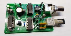
Well, you won't believe it ... but I have found yesterday that I had developed, a few years ago, a board with:
-TTL and SPDIF inputs
-BNC and ST outputs
see the attached photo !...
I still have to find the schematics and PCB in my files, but it is there...
It uses an AVAGO HFBR-1414TZ emitter, because I intended to use it on the modified input of the Wadia (the input having an Avago receiver).
I still have to test my board because I do not remember if my engineer or myself (a friend of mine) had tested it ...
Assuming that this board works OK, my project would be to:
So my first question is:
-suppose that I have a BNC source, can I connect the BNC signal directly to the SPDIF input, or should I add some specific parts between the BNC source and the SPDIF input of my board (or any other board supposed to undertake SPDIF signals) ? I ask this because I am not 100% sure that a BNC input signal is a SPDIF signal ...
-TTL and SPDIF inputs
-BNC and ST outputs
see the attached photo !...
I still have to find the schematics and PCB in my files, but it is there...
It uses an AVAGO HFBR-1414TZ emitter, because I intended to use it on the modified input of the Wadia (the input having an Avago receiver).
I still have to test my board because I do not remember if my engineer or myself (a friend of mine) had tested it ...
Assuming that this board works OK, my project would be to:
- have a BNC + Toslink inputs
- if not too complex, have also an AES/EBU input
- I will use the existing BNC and ST outputs in a first time, and will try to add a Toslink output when everything else works.
So my first question is:
-suppose that I have a BNC source, can I connect the BNC signal directly to the SPDIF input, or should I add some specific parts between the BNC source and the SPDIF input of my board (or any other board supposed to undertake SPDIF signals) ? I ask this because I am not 100% sure that a BNC input signal is a SPDIF signal ...
Sorry for my English, but I do not understand very well what you mean: can you show an example of such a board ? is a Toslink output signal a TTL signal (so I could send it directly in my board or any other board supposed to undertake TTL signals ) ?For a TOSLINK to ST board just buy a $7 one in three out TOSLINK switcher to use for modding.
Attachments
https://www.ebay.com/itm/254698715772
yep
Whats the bet you keep using the wrong ST brand so you can keep finding out its a bad fit?
If you really want to try and take the Wadia 9 to the next level
1. Do a J-test with ST input - optical jitter can be bad unless a good PLN sored that
2. If the jitter is bad
3. scope the ST optical board digital outs to work out if its I2S or right justified and the voltages
4. Remove the optical board and use a super low jitter USB to I2S /PCM from iancanada
profitez du voyage
Auvoir
Doesn't the Wadia have its own clocks? If so, and if its only inputs are optical SPDIF, then seems like it must be doing ASRC or FIFO already?
Of course the Wadia will have its own clock and will have some Async SR converter to cope with jitter related problems.Doesn't the Wadia have its own clocks? If so, and if its only inputs are optical SPDIF, then seems like it must be doing ASRC or FIFO already?
And since ST fiber transmits nothing else but SPDIF, all that Nounours needs is the very simple Avago schematic from their application note, where even a PCB proposal was given.
Input is just a BNC signal terminated with 75R.
And also keep in mind that ST is a standardised protocol. No need to have matched transmitters and receivers.
Hans
Nice!Well, you won't believe it ... but I have found yesterday that I had developed, a few years ago, a board with:
-TTL and SPDIF inputs
-BNC and ST outputs
see the attached photo !...
Where will the BNC input signal come from? If it's a CD player or transport then it's almost certain to be a SPDIF signal already.... SPDIF is the standard output signal for these things.... If the output is a RCA you can add a RCA to BNC adapter.So my first question is:
-suppose that I have a BNC source, can I connect the BNC signal directly to the SPDIF input, or should I add some specific parts between the BNC source and the SPDIF input of my board (or any other board supposed to undertake SPDIF signals) ? I ask this because I am not 100% sure that a BNC input signal is a SPDIF signal ...
The only other types of output (other than SPDIF) you're likely to (rarely) find on hifi equipment is I2S (which won't use a BNC/RCA connector), a clock signal (should be labelled something like WCLK - don't use this as input to your board), or a SDIF-2 or 3 connector (very rare - usually only DCS gear has this, and again will be labelled and in a group of at least 2 connectors).
If you're thinking of using a BLU Ray/DVD or games console as a source then you may need to configure the output type in the menu (e.g. to PCM) - I don't use these for this purpose so don't know 100%, but I'm sure it can be made to work.
...
I agree there may be different objective & perceived quality from different brands of transmitters/implementations etc. The circuits are so simple you can build multiple with different parts and see what you like best. The power supply may also affect performance - again you can experiment.
Last edited:
the spec for s/pdif over BNC (AES3id) is 1.0Vpp, while s/pdif RCA is min 500mV.
Rane RaneNote149 describes the various AES3 and s/pdif electrical signaling standards as well as adapters to convert from one type to another. BNC input to RCA output adapter won't work (ideally or if at all) the other way around as it is a signal attenuator.
Ability of an RCA s/pdif output to drive a BNC AES3id input will vary depending on the specific (often non-standard) implementation of the source and receiver hardware to ensure adequate signal transition threshold and noise margin.
Last edited:
I should clarify when I said "adapter" for the output I meant one like below (rhs) that has no attenuation and is simply used to convert one plug type to the other...

My preference is not to use an adapter however.
My preference is not to use an adapter however.
@Nounours,
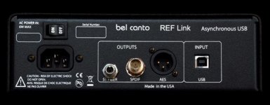
You have a reflink with ST and BNC output.
Look inside your reflink and you see how both are made from one signal. It also gives you the answer how to go from BNC to ST.
Hans
You have a reflink with ST and BNC output.
Look inside your reflink and you see how both are made from one signal. It also gives you the answer how to go from BNC to ST.
Hans
Thank you very much for replies ! I must study them a bit to understand them and define the priorities...
First of all, forget everything related to RCA: when it comes to digital, I don't care at all about RCA that is stupid (non musical) Financial Director choice; it has zero interest for me.
I had developed my board with an Avago because a few years ago I believed that the Avago will give
better results on the W9 than the stock CTS; but it seems to be the opposite.
I can change the Avago for a CTS later, I mean after the board works OK: it will not be a big challenge to adapt the PCB.
@kazap: thank you for the Toslink splitter: I will buy one soon , preferably from Europe (if available) to avoid custom taxes...
My plan is too make the test with the Avago, just to be sure that the board works, because I don't remember to have tested it !
When it works, I have 2 options: Keep the Avago and connect it to the Avago input of the W9, OR design a new PCB to host the CTS.
The 1st thing I have to perform is to test if the board works !
I have a laboratory P.S., so I can easily feed it with 5V.
I also have a scope and a signal generator: so it should be possible to inject a signal into the (SPDIF or TTL) input and measure the output at the BNC output. Less intuitive regarding the ST output test...
But for this very first test, I need some guidance !
I have designed a lot of electronic things and a lot of PCBs, but I am not good enough regarding this kind of tests...
First of all, forget everything related to RCA: when it comes to digital, I don't care at all about RCA that is stupid (non musical) Financial Director choice; it has zero interest for me.
No: the Reflink does not have a BNC input: is has only a USB input, and BNC/ST/AES-EBU outputs: see attached photo.@Nounours,
You have a reflink with ST and BNC output.
Look inside your reflink and you see how both are made from one signal. It also gives you the answer how to go from BNC to ST.
Yes: the purpose of my board (that is exclusively oriented towards Audio) is to receive the signals from Drives/CD transports, so I understand (based on what you say) that these signals should already be SPDIF, so they should be undertaken by my board (it is supposed to undertake SPDIF or TTL).Where will the BNC input signal come from? If it's a CD player or transport then it's almost certain to be a SPDIF signal already.... SPDIF is the standard output signal for these things.... If the output is a RCA you can add a RCA to BNC adapter.
I agree; not my first priority but interesting information.If you're thinking of using a BLU Ray/DVD or games console as a source then you may need to configure the output type in the menu (e.g. to PCM) - I don't use these for this purpose so don't know 100%, but I'm sure it can be made to work.
I agree again, and I know how to build very good P.S. (I have already built a lot of them and upgraded a lot of stock P.S.), so I know their impact on the sound.I agree there may be different objective & perceived quality from different brands of transmitters/implementations etc. The circuits are so simple you can build multiple with different parts and see what you like best. The power supply may also affect performance - again you can experiment.
I had developed my board with an Avago because a few years ago I believed that the Avago will give
better results on the W9 than the stock CTS; but it seems to be the opposite.
I can change the Avago for a CTS later, I mean after the board works OK: it will not be a big challenge to adapt the PCB.
@kazap: thank you for the Toslink splitter: I will buy one soon , preferably from Europe (if available) to avoid custom taxes...
I don't understand clearly (sorry, my English is not perfect)Whats the bet you keep using the wrong ST brand so you can keep finding out its a bad fit?
My plan is too make the test with the Avago, just to be sure that the board works, because I don't remember to have tested it !
When it works, I have 2 options: Keep the Avago and connect it to the Avago input of the W9, OR design a new PCB to host the CTS.
I understand what you mean, but this is beyond my knowledge: I don't to proceed without guidance.If you really want to try and take the Wadia 9 to the next level
1. Do a J-test with ST input - optical jitter can be bad unless a good PLN sored that
2. If the jitter is bad
3. scope the ST optical board digital outs to work out if its I2S or right justified and the voltages
4. Remove the optical board and use a super low jitter USB to I2S /PCM from iancanada
The 1st thing I have to perform is to test if the board works !
I have a laboratory P.S., so I can easily feed it with 5V.
I also have a scope and a signal generator: so it should be possible to inject a signal into the (SPDIF or TTL) input and measure the output at the BNC output. Less intuitive regarding the ST output test...
But for this very first test, I need some guidance !
I have designed a lot of electronic things and a lot of PCBs, but I am not good enough regarding this kind of tests...
Attachments
If the board has SPDIF in that works, and the objective is to connect it to a CD transport via BNC cable, then I would initially go about it as follows
1. Get a 75ohm BNC connector
2. Build the extremely simple circuit from post 22 above (75R resistor, 4.7nF capacitor - cap value can be different if you don't have 4.7nf to hand)
3. Wire BNC in > circuit from post 22 (75R & 4.7nf) > SPDIF in on your board
4. Connect a CD player/transport digital out see if it works
Assuming that your board works that should be all required... If your board already has the circuit from post 22 at the input then don't add it again.
to test your board (which has s/pdif input and BNC output);
set scope input channels to DC coupling, High-impedance mode (1-10 Meg Ohms OK if using 10x probe), turn bandwidth BW limiter off, set triggering to auto level, etc.
set signal generator to square wave, 6MHz (or as close to this as possible, ~1 MHz OK) 50% duty cycle, 600mVpp, 0 DC offset (waveform should cross 0V symmetrically)
connect signal generator to input of your board directly (no rc network needed)
your board's BNC output should be same square wave waveform, but with 1.0Vpp amplitude (or possibly 2.0Vpp depending on implementation) when driving the scope's hi-impedance load.
you may need to increase the signal generator amplitude to 1.0Vpp if no signal at the BNC output
if this works, then board is probably OK, so connect CD player s/pdif digital output to your board, and board ST output to the Wadia ST input.
from a brief look at the Avago datasheet, there are several models of the ST transmitters and receivers, it looks like they are factory graded or tested to operate at certain data rates. the external passive component (resistor and capacitor) values are dependent on the transmitter / receiver characteristics and also the data transmission rate.
Read my posting again, I was talking about ST and BNC output, not input.No: the Reflink does not have a BNC input: is has only a USB input, and BNC/ST/AES-EBU outputs: see attached photo.
And I mentioned that both output signals where made from the same signal, confirming to you that ST uses just as well the SPDIF protocol.
For your solution, depending on the Avago transmitter, all you have to do is a level adjustment from a 75R terminated BNC signal.
Don’t make things more complex as needed.
Hans
Well, I have spent a few hours to draw back the ST output part: see attached file.
The way the HFBR 1414TZ is connected differs from the official Avago diagram, but I know that this diagram had been optimized to use the 74AC14 circuit.
I have not found more information for the time being.
Have you already seen this diagram with these parts' value ?
I know that it had been published in specialized websites a decade ago, but I have not managed to find it again.
Attachments
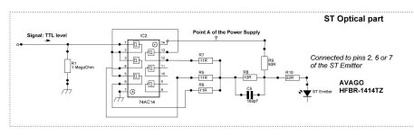
Parts of your drawing are reminiscent of the TX circuit in the datasheet but it's not the same - https://docs.broadcom.com/doc/AV02-0176EN
If you have reason to think it's a good design that has been optimised then what is stopping you trying it?
If you have reason to think it's a good design that has been optimised then what is stopping you trying it?
for your circuit using the 74AC schmitt trigger hex inverters, unused inputs (pins 9 & 11) should not be left floating but should be tied to pin 7 (ground).
while both your ckt and the Broadcom reference should work, note that absolute polarity on the broadcom reference schematic is inverted vs yours (broadcom ckt logic "1" input turns IR emitter off). shouldn't make a difference with an NRZ signal, which s/pdif is. Rough calculations show about 80mA steady-state "LED on" current for each circuit.
more interesting to me is the remainder of the circuit, which hopefully will be able to convert a BNC s/pdif signal (1.0Vpp, 0 DC average level) into a TTL level to drive the 74AC portion shown.
Last edited:
Yes you are right, I know that, and as far as I remember, this circuit was an "upgraded" version of the Avago circuit: but I cannot find where I got it at the time...Parts of your drawing are reminiscent of the TX circuit in the datasheet but it's not the same
Mainly because the board has no regular input connectors for SPDIF and/or TTL: so I will be obliged to solder some wires directly onto the board holes, that is not very clean..If you have reason to think it's a good design that has been optimised then what is stopping you trying it?
And secondly because I try to verify as many details as possible before proceeding with a test...
you are totally right ! I have checked both the schematics and the board itself:for your circuit using the 74AC schmitt trigger hex inverters, unused inputs (pins 9 & 11) should not be left floating but should be tied to pin 7 (ground).
- the pins 9 &11 are not linked to GND on the schematics,
- but they are connected to the ground on the board,
What could be the impact if these pins would be floating ?
you are right again, but I remember that I had been told that it was the best way to engineer it.while both your ckt and the Broadcom reference should work, note that absolute polarity on the broadcom reference schematic is inverted vs yours (broadcom ckt logic "1" input turns IR emitter off). shouldn't make a difference with an NRZ signal, which s/pdif is.
Let's say 200mA, so one of my high-end power supply should be a perfect match: they are theoretically able to deliver up to 1A.Rough calculations show about 80mA steady-state "LED on" current for each circuit.
I work on it...more interesting to me is the remainder of the circuit, which hopefully will be able to convert a BNC s/pdif signal (1.0Vpp, 0 DC average level) into a TTL level to drive the 74AC portion shown.
This is also a "must have" for me, because my main goal is to have a ST output (which requires a TTL level at its input).
Except the Toslink input that will generate a TTL level (its signal output is TTL level if I am right), a BNC input would be a SPDIF level : correct me if I am wrong.
So I currently design a new PCB that will have all the standard input connectors (2xBNC, 1xToslink, 1xAES/EBU, maybe an I2S input if I have time to understand it, and a ST input but not required for my own usage) and the standard outputs connectors (1xBNC and 1xST) already present on the existing board.
This new PCB re-use the existing board we are talking about, and will have the abovementionned inputs with the proper onboard connectors.
I have already built the 5V power supply to feed all these folks.
The priority remains to test the existing board, which sadly does not have the clean input connectors.....
there are two other IC's plus other parts, what IC's and how are they connected? I recommend testing that circuit as-is by soldering some wires from the pcb holes to an off-board connector to verify the functionality of the circuit, then after its debugged, design another board with pcb-mount thru-hole connectors.

- Home
- Source & Line
- Digital Source
- BNC (or Toslink) to ST interface