Hello members, 
actually I work on my first LM3886 Amp and for this I want to have also a subwoofer filter.
So I have later a 2.1 System.
I found this and I be very interessed on it:
https://www.lcaudio.dk/pdfs/subfilter.pdf
Does anybody build and make this in this way by EasyEda or KiCad an want to share
the PCB Gerber Data with a young electronic interessted girl ? 😉
I want to test it, and it was on first step easier to get a finished PCB
for testing and understanding.
kind regards
Before going for something that complex, so read Rod Elliot on why a phase adjustment may not be the most useful.
My subs, I only build critical Q sealed, I do not need a HP filter as I don't reach X-max until 10 Hz @ 105 dB, so never going to happen. I run LR-4 crossover.
As I did not want to build my own boards, I use the ones from X-Kitz. If you do have a ported sub, useless IMHO, then you need a HP filter too.
You can figure out what you need with programs like WinISD.
You could build that on a solderless breadboard in an hour or so. And you could even reuse the parts- no soldering.I want to test it, and it was on first step easier to get a finished PCB
for testing and understanding.
https://www.amazon.com/RSR-Solderle...ocphy=9018935&hvtargid=pla-642540929164&psc=1
thanks for the praise 😊😍Some kids are pretty darn smart.
Last edited:
Yes , of course, but I thing then i get bad results.You could build that on a solderless breadboard in an hour or so. And you could even reuse the parts- no soldering.
https://www.amazon.com/RSR-Solderle...ocphy=9018935&hvtargid=pla-642540929164&psc=1
Because of long wires.... ESL , OPAs could go swinging and so on.
But the Idea was good, but for Audio and OPas I thing not practicable.
In the past I do so with other Digital stuff....
I write now a Email to Mr. Clausen and ask for help.
I would like to test and understand the technology, the behavior etc...
So I never question whether it makes sense. Of course it makes sense to learn something that is technically possible.
It's about learning through practice... not just buying.
👌🌞
Not at all, I have breadboarded many high frequency circuits with good results for many years.Yes , of course, but I thing then i get bad results.
Because of long wires.... ESL , OPAs could go swinging and so on.
Just take a little care and understand the circuit layout. This saves much time, several board revs,
and the time and material costs.
And you can move the through hole parts from the breadboard to the pcb when you finish it.
I do breadboard debugging with through hole parts, even for boards that will use smt parts,
since hand assembly of smt boards is extremely time consuming. Of course the layout will
change and in general be improved with the smt pcb.
Last edited:
soNot at all, I have breadboarded many high frequency circuits with good results for many years.
Just take a little care and understand the circuit layout. This saves much time, several board revs,
and the time and material costs.
And you can move the through hole parts from the breadboard to the pcb when you finish it.
I do breadboard debugging with through hole parts, even for boards that will use smt parts,
since hand assembly of smt boards is extremely time consuming. Of course the layout will
change and in general be improved with the smt pcb.
rayma
your words in my mind.... I will test it, because i have exact this board here 🙂
also the NE5532 and some Rs and Cs.... because of testing LM3886
I try OPA modul per OPA modul and then I see the result.
....and woe, woe, if that doesn't work😉
Just follow good practice, similar to how you would lay out a pcb. Minimize the high impedance nodes.
Short leads. And use local decoupling. Double check all connections before applying power.
Pins on an IC are numbered CW as viewed from the bottom, so they are CCW as viewed from the top.
Remember that problems are an opportunity to learn, and that's always a good thing, esp for a young person.
If you just solder a pcb designed by someone else, you don't really gain any more useful knowledge.
The journey is the destination. Etc. etc.
Last edited:
👍Just follow good practice, similar to how you would lay out a pcb. Minimize the high impedance nodes.
Short leads. And use local decoupling. Double check all connections before applying power.
Pins on an IC are numbered CW as viewed from the bottom, so they are CCW as viewed from the top.
Remember that problems are an opportunity to learn, and that's always a good thing, esp for a young person.
If you just solder a pcb designed by someone else, you don't really gain any more useful knowledge.
The journey is the destination. Etc. etc.
Dear
so I build, measure and now understand .... good tip , I never come to the idea, but mostly , the simplest is so near.
Many Thanks.
I also get answer from Mr. Clausen, a fine man.
He know nobody that has ever build his draft.. Iám the first one, he mentioned.
rayma,
your tip was great... I test each "modul" by own.... fine ! only in togehter it do not works fine by ear. but on Oszi I see all in sinus Test curves.so I build, measure and now understand .... good tip , I never come to the idea, but mostly , the simplest is so near.
Many Thanks.
I also get answer from Mr. Clausen, a fine man.
He know nobody that has ever build his draft.. Iám the first one, he mentioned.
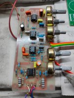
WOw, fine.....so nice work.Very rough working design .
warm regards
Andrew
You are very fastv , faster as I.
I have also make it on a breadboard, but very noise.
Dear andrewlebon, do you wnat to share the gerber Data with me, so I can make it for me and do all the Test for learning for me .
What do you think about that ... please please 😍

So because of no feedback🙄 and others will not to share it to members I done my own. 🙂
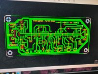
Perfect but in SMD and very very stable and so good behaivior in case of disortaion.
Don´t wonder about trimmer, i had only single to hand , but works perfect to adjust...
PCB = 4 Layer with inner GND.
Top and Clear results ... Fine
Perfect but in SMD and very very stable and so good behaivior in case of disortaion.
Don´t wonder about trimmer, i had only single to hand , but works perfect to adjust...
PCB = 4 Layer with inner GND.
Top and Clear results ... Fine
Attachments
- Home
- Source & Line
- Analog Line Level
- Help needed by building a subwoofer filter and looking for a possibility of a sharing Design for testing