You missed "noise floor modulation" effects, invisible on a FFT, "time variant" effects, etc... almost all reported by a "professional audio designer friend" with alleged no vested interest in spreading FUD.However in contrast to quantum world in audio the uncertainty principle has one exception: close-in phase noise. So the lower the close-in phase noise the better it sounds regardless of anything else.
"professional audio designer friend"
 Uh, you missed "full time" in front of it. It may be a short phrase but it does carry a different tone in the discussion.
Edit: Oops, it's "full time ... high end" in front. Sorry.
Greetings. Forgive me if this was mentioned somewhere in the depths of this thread but I cannot find it.
Does anyone know the expected frequency content at the AVCC, VDD, DVDD, and AVDD pins?
It's difficult to design regulation without knowing what I'm filtering.
Also which ones take priority in filtering? The AVCC is obviously the most critical but the rest are a bit more obscure in what they do.
I have no idea what the circuits that VDD and DVDD drive actually do and the AVDD is said to be for the oscillator and the gain compensation, however if an external XO is used then it is only for gain compensation.
It is difficult to know which supplies are more important to filter and what frequencies are present at each.
Your wisdom would be appreciated.
Filtering? For ES9038Q2M?
IIRC, Vdd uses in internal regulator and the datasheet recommends a particular filter cap. Actual cap is not too critical IME just so long as its good enough.
Regarding VCCA, even if using an external clock there may be internal clock buffering and distribution that benefits to some degree from low noise on the power rail. Just saying I wouldn't assume that rail isn't important without experimental confirmation.
With the exception of AVCC, all the other dac power rails usually work fine with standard decoupling practices (e.g. .1uf X7R and 10uf tantalum close as possible to the load). If optimal performance were sought, I would use a separate regulator for each rail. For lowest cost some designs use a single regulator. In the latter case sometimes ferrite beads are used for additional isolation, a practice I would personally rather avoid if possible (since ferrites can produce hysteresis noise that is hard to make sense of on FFT yet which can in some cases affect SQ; if doubtful I would suggest to try it both ways and see what you think).
Regarding frequency range of noise on each rail, its hard to say exactly. Clock edge noise can extend up to several hundred MHz if not higher. Easy to see with an E-field probe and spectrum analyzer that dac chips produce extremely broadband noise locally.
Regarding AVCC, depending on how well everything else in the dac and the reproduction system are designed, almost any change in AVCC regulation or filtering can be audible. So, pick something you like the sound of if this is going to be for a listening dac. If a measurement dac then just use whatever measures well.
Hi guys - have been reading through some of this thread, as I'm currently in the process of extensively modding a yamaha cx-a5100 ATMOS preamp...
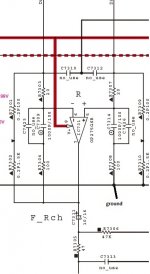
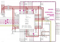
The a5100 uses a ES9016 ultra DAC, so a bit different that the stero DAC used here. Interestingly, due to the increased current requirements it uses an opamp to drive a transistor with a 5V source to derive the 3.3V - I've attached the schematic. I also got my hands on the a5200 schematic today and it interestingly has unpopulated IC and associated components for a regulator which they seem to not have implemented in favor of keeping the opamp circuit (attached circuit is actually the a5200 one but exactly the same as a5100).
I've attached it here in case it inspires anyone for chips that require more AVCC current, etc..
Now, the opamp circuit has minimal decoupling, uses a NE5532 rather than the LME49720 used here and uses a 5V source that seems to be a system wide used rail so there seem to be areas of potential improvement.. Planning on using a LT3045 regulator based circuit from LDOVR to supply the 5V, swap the opamp to a LME49720, and add a bunch of decoupling... also planning to swap the resistors to thin films...
Any suggestions or criticisms are very much appreciated..
Attachments
We eventually settled on OPA1612 op amps as the best sounding for the dacs in this thread. That's also what ESS now uses in their eval boards, and what AKM used for AK4499 eval board. A possible problem with LME49720 is that it is IIRC a rebranded LM4562. Those op amps have been known to be particularly sensitive to RF at the inputs, and some places in dacs have a lot of RF. Topping did use LME49720 for D90 output drivers, but I/V and IIRC differential summing stages were OPA1612. Seems to me some LM4562 also had reported problems with popcorn noise.
Regarding voltage regulation, probably best to have one dedicated 3.3v regulator for each AVCC rail (AVCC_L and AVCC_R). Some people use unbuffered op amps for that if they can supply enough current. Its also important that the AVCC regulators have a very low impedance path to the AVCC pins.
There is much more that could be said about getting the best sound out of ESS dac chips, but some of it maybe not worth the effort if hacking an older dac design.
Last edited:
Perfect - thanks very much Mark!
I'm amend the planned design then to use the OPA1612 - I was using post 3003 schematic which was referenced a few pages ago.
Unfortunately the PCB design is going to preclude using separate supplies for each side - and in fact the supply is supplying two 9016 chips. The DAC side of the circuit is attached here (again from the 5200 given it is the same aside from ES9026 vs ES9016 since the PDF is better) - it uses a ferrite at the insertion point to the DACs 4 AVCC inputs, and uses a local 100uf Tantalum cap for supply decoupling, then 0.047uf local (I think per the parts list) mylar caps. I was going to swap the 100uf tantalums for 100uf mlcc ceramic with a 0.1uf and 100pf in parallel.. Not certain what to do about the ferrite..
IV stage is attached as well - I've swapped the NE5532 for OPA1656 as well on that and added additional local decoupling. This design immediately switched the balanced 9016 output to SE output - I've then taken the signal off of this stage and sent it to a neurochrome universal buffer for SE-->Balanced conversion then built a 9 channel Muses 72323 based external volume control to bypass the inbuilt crappy volume IC... so I've gone to pretty substantial ends to improve performance, and actually quite interested in whatever optimization...
Thanks a lot
Vic
Attachments
Yup, very true and a thought I just had too.. That would at least allow the seperation of the AVCC supplies between the two DACs - I had actually bought a second LDOVR LT3045 board at 3.3V output in case I wanted to use it.. maybe it would make sense to power the less critical DAC (which does some of the surround channels) directly with that and then beef up the main supply to the primary DAC as above..
Or alternatively I power both independently with each LT3045 and swap the resistor on the 5V board to configure it to 3.3V instead.. maybe this is the lesser of all evils?
Or alternatively I power both independently with each LT3045 and swap the resistor on the 5V board to configure it to 3.3V instead.. maybe this is the lesser of all evils?
Last edited:
Personally, I never liked super LDO regulators for AVCC. Opamp regulators usually sound better to me. ESS recommended opamp regulators for AVCC sometime back in or around the beginning before their dac chips needed more current than an opamp could supply. Also, IIRC Topping used opamp AVCC regulators for the newest version of D90, the one with an ESS chip. Best of all would probably be some discrete regulator that could be more exactly optimized for the load. The other thing about AVCC regulators is that I personally wouldn't want to connect a nonlinear C-2 or C-3 ceramic cap to AVCC. A regulator that needs an output cap of that type would be something I would probably try to avoid. That's not to say you shouldn't try it and see what you think yourself. I would only suggest to compare the sound with different regulators and pick one you like.
Fair enough, much appreciated.
So the main thing then is that presumably the typical opamp regulator didn’t supply enough current to adequately power the circuit (which would be supported by the findings referenced earlier in this thread: https://www.diyaudio.com/community/threads/es9038q2m-board.314935/page-62#post-5442900), which would be why they went with the topology they went with with the opamp controlling the transistor 5V output to regulate to 3.3V. So question will be is this better than the LDO regulator (especially if I run the less critical DAC separately) vs LDO for each.. understood re: the caps..
So the main thing then is that presumably the typical opamp regulator didn’t supply enough current to adequately power the circuit (which would be supported by the findings referenced earlier in this thread: https://www.diyaudio.com/community/threads/es9038q2m-board.314935/page-62#post-5442900), which would be why they went with the topology they went with with the opamp controlling the transistor 5V output to regulate to 3.3V. So question will be is this better than the LDO regulator (especially if I run the less critical DAC separately) vs LDO for each.. understood re: the caps..
Which dac chip is in your dac? ES9038PRO?
EDIT: Also as I said, I wouldn't use an high performance LDO for AVCC. Tried it before and didn't like the sound. Loading the LDO with a resistor to ground helped some, but still not very good sound to me. Again, I suggest people try it and see what they think. You wouldn't be the first person who tried an LT3045 and then decided an opamp or a Jung regulator sounded better in their opinion. Why that has turned out to be the case for some people is not something that has been studied, at least not that I know of.
EDIT: Also as I said, I wouldn't use an high performance LDO for AVCC. Tried it before and didn't like the sound. Loading the LDO with a resistor to ground helped some, but still not very good sound to me. Again, I suggest people try it and see what they think. You wouldn't be the first person who tried an LT3045 and then decided an opamp or a Jung regulator sounded better in their opinion. Why that has turned out to be the case for some people is not something that has been studied, at least not that I know of.
Last edited:
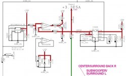
Two 9016 ultras - all 8 channels in use in each..
https://usa.yamaha.com/products/audio_visual/av_receivers_amps/cx-a5100_black_u/index.html
https://usa.yamaha.com/products/audio_visual/av_receivers_amps/cx-a5100_black_u/index.html
Page 24 of ES9016S Datasheet says nominal AVCC_L and AVCC_R current is 25mA, so for all 8-channels in one chip it would need roughly 50mA (assuming operating conditions are similar to those ESS specifies). Some opamps could handle that without a buffer transistor and others might need one.
Yeah fair enough.. what was giving me some pause was the discrepant much higher current requirements discussed re: a 9028pro vs the datasheet so wondered if similar might be an issue here.. However on re-reading that article it was the 1.2V rail that was pulling more current..
http://www.dimdim.gr/2017/05/es9028pro-power-wows/
http://www.dimdim.gr/2017/05/es9028pro-power-wows/
Also re: the LDO I definitely understand what you’re saying and appreciate the feedback. I think given this conversation if I was to run one DAC off of one it would be the one doing the cieling atmos surrounds which I’m not sure I’d hear a difference in anyways given their caliber of speaker in my setup vs the fronts which are elsinores.. but maybe I would.. Problem is space is at a premium so trying to come up with a way to practically optimize the critical component performance..
Okay, so to give some headroom for the ES9016 ultra current requirements, maybe I could use either:
OPA1656 - 100mA output: https://www.ti.com/product/OPA1656
OPA1622 - 145mA output: https://www.ti.com/product/OPA1622
I happen to have a bunch of 1656s hanging around... any reasons to think it wouldn't be a reasonable choice here for AVCC?
Thanks a lot again!
OPA1656 - 100mA output: https://www.ti.com/product/OPA1656
OPA1622 - 145mA output: https://www.ti.com/product/OPA1622
I happen to have a bunch of 1656s hanging around... any reasons to think it wouldn't be a reasonable choice here for AVCC?
Thanks a lot again!
Last edited:
What are you looking for from us? The link you posted is talking about the core voltage needs increasing, not AVCC and it is talking about a board running 100MHz clock, with a 9028, which requires higher current in both cases (9028 is higher than 9018, which is again higher than 9016 and 100MHz will be higher than your board by quite a margin I would think). So, what is the XO frequency for your 9016 board? That will govern what is needed for core voltage.
Also, the 'inbuilt crappy volume IC™' is the dac itself and unless you are using an amplifier with far too much gain for your needs, then there is nothing crappy about it. I would expect you to get worse results with the MUSE, rather than better if gain structure is respected.
Also, the 'inbuilt crappy volume IC™' is the dac itself and unless you are using an amplifier with far too much gain for your needs, then there is nothing crappy about it. I would expect you to get worse results with the MUSE, rather than better if gain structure is respected.
Last edited:
What are you looking for from us? The link you posted is talking about the core voltage needs increasing, not AVCC and it is talking about a board running 100MHz clock, with a 9028, which requires higher current. So, what is the XO frequency for your 9016 board?
I was hoping maybe that someone had experience with using the 1656 when people were investigating alternatives to the original LME, but perhaps not..
The other thing is reading the ES9016 datasheet - there are two separate pins for AVCC L and R each - 4 input pins. The above 50mA assumption was based upon doubling the current requirement based on 2 supply pins - L and R but I’m not certain if they’re internally connected or not.. so possibly if not then if the datasheet is indicating 25mA x4, then 100mA is the requirement hence a higher output opamp.. which is why I had found a couple possibilities to ask about from people in the thread that have more experience with the circuit. Also the datasheet has the same clock and sampling frequency footnote tied to VDD, DVCC and AVCC, so seems to be indicating all 3 may depend upon not only clock rate but sampling rate of the supplied signal..
EDIT:
The volume IC used in the Yamaha cx-a5100 is not the DAC - it is a BD34703KS2 which follows the DAC and regulates the volume coming from both analog and digital sources downstream of the DAC.. as well as level controls between speakers.
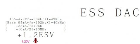
I also found a comment on the 1.2V rail regarding differential clock and sampling rates and seemingly power supply draw dependent on these factors. Its attached.
Attachments
Last edited:
the 1656 has been used extensively for IV conversion, but not so much in buffered references. I hold a different opinion to Mark regarding the use of opamps this way. I would not expect the 1656 to be terribly happy with such a high capacitance load, but by all means give it a try. No, there are not 4 x 25ma ... look at the way the current output is specified. AVCC supplies the current output. yes, they all depend to some degree on the clock frequency and sample-rate, but none as directly as the core digital voltage. exactly how much, you will need to find out experimentally, so just design with some margin.
- Home
- Source & Line
- Digital Line Level
- ES9038Q2M Board