I derived the title of this thread [Analog Pulse Line Level] from this Forum's title of [Analog Line Level].
Its objective is to add a different food and fiber for thought and analysis. .
1. Analog Pulses are generated from the precise rectification of Analog Signals.
2. Analog Pulses are processed/amplified in DC circuits.
3. Analog Signals are lastly reconstiuted from their Analog Pulses.
This approach to processing works. Please use the thread [as reference] which is entitled "Class aP amplification" in the Pass Labs Forum.
Anton
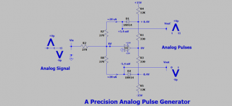
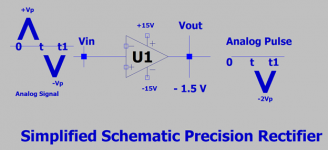
A precision analog pulse generator [the circuit; part 1]
The schematic of the subject is attached. The following are its salient properties to focus on:
Model Analog Signal input to the generator.
1. Positive and negative parts have equal peak amplitudes [+/-Vp].
2. The time stamp [0 t] for its positive-going and [t t1] for its negative-going parts.
Must keep track of the above vector stamps is the message. Easy to accomplish.
Analog Pulses. The Op amp circuit used rectification as the scalpel to cut the input Analog Signal along its time axis [0 t t1] to give the two output and fully separated pulses. Continue tracking their time and peak amplitude vector stamps.
This rectification is precise; meaning repeatable; but may or not be accurate or faithul in generating exact output replicas of the parent Analog Signal.
Circuit. In general;
1. Op Amp inverts phase. By example the positive-going part of the input analog signal [0 to t] is now negative-going.
2. Any Op Amp [integrated and discrete] and switching small signal diode [Si and Ge] are acceptable.
3. The +/- 15 V power rails feeding the circuit may be lower. I see Op Amp characteristics suggesting voltage rails like +/-2.5 V.
4. I use 1% metal film resistors
This attached circuit has the following especific requirements:
1. 1N914 is a Silicon diode.
2. The voltage divider [12 K + 330 Ohm] grants by example the upper 1N914 [+0.4 V] to forward bias it Class AB; as suggested by the ~20uA current flowing thru it.
3. Lower the value of the 12 K resistor in the voltage dividers to 2.4 K when using +/-3 V instead of +/-15V for system PSU. So as to attain the same shown quiescent condition.
4. Did you notice that the outputs bear a DC offset of +/-5.4 mV; from Ohms's Law [270 Ohm X 20 uA]?. Higher valued DC offset [say +/-0.7] can be readily attained and useful in other future circuits.
How's it work is next
Attachments
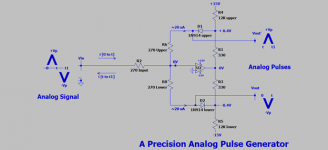
Operation of a precision analog pulse generator.
The attached schematic of a precision analog pulse generator [or a precision rectifier] is the same as the one I showed in the previous post. But with the following add ons for clarification:
1. The labels UPPER and LOWER on resistors and diodes.
2. The input current [i 0 to t] flowing thru the 270 Ohm input resistor from the positve-going component of the input Analog Signal. Note its direction per convention; from positive potential to zero at the inverting input of the OpAmp. Ditto for the input current[i t to t1] from the negative-going component of the input Analog Signal. Note its direction which is in the opposite direction per the same convention.
Rectification
1. The positive-going component of the input Analog Signal pushes its current [i 0 to t] thru resistor 270 input towards the inverting input of the Op Amp. Can't go thru; because this port has a high input impedance and this current simutaneously attempts to raise its voltage to above zero. So
2. The Op Amp drops its output voltage to a value lower than its quiescent of zero [say to -0.1 V at peak] so as to divert this input current [i 0 to t] thru the 270 Lower resistor, thru the diode 1N914 lower and thru 12 K lower thru the -!5 V rail to ground [common] to its origin.
2.a The negative-going Analog Pulse [0 to t] is thus generated across the 270 Lower resistor [Ohm's Law]
2.b The diode 1N914 Upper stops conducting [cuts off] because the new output voltage of the Op Amp which now equals [-0.1 V] is subtracted from its quiescent [+0.4V] to the new value of [+0.3 V].
3. The current [i t to t1] is demanded by the negative-going component of the input Analog Signal. The inverting input of the Op Amp does not have it; by example it can be the gate of an FET. The negative-going voltage of input Analog Signal simultaneously attemps to lower the quiescent voltage of this port to below zero.So
3a. The quiecent output voltage of the Op Amp rises from 0 V to [say +0.1 V].
3b. This new output voltage adds to the forward bias [0.4 V] voltage of the diode 1N914 Upper to [+0.5 V] causing it to conduct further. Simultaneously cuts off diode 1N914 Lower per [+0.1V -0.4 V = -0.3 V]
3c. The current [i t to t1] flows from +15 V [by convention] thru 12K upper thru diode 1N914 Upper thru resistor 270 Upper thru resistor 270 input thru Analog Source to common.
3d. The positive-going Analog Pulse [t to t1] is generated across resistor 270 Upper.
Best
Anton
Attachments
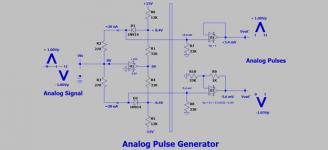
Hello,
The attached schematic expresses the ability of [Precision Rectification] to modify, and/or distort the input Analog Signal; but with a specific objective. The part of the schematic which is to the left of the double line vertical barrier is the same as I showed in the previous posts. Please note the following changes:
1. The Analog Pulses [Vouts] of the left side sub-schematic are buffered with OpAmps in the right-side sub-schematic.
2. Note that the Analog Pulses Vout levels are loaded by equal 33 K resisors for the upper and lower buffer circuit at the OpAmps' non-inverting inputs. Not needed anyway and can be ommited. But the message is do not disturb the intrinsic operation of the precision rectifier by preserving its built in symmetry. Play with one variable at a time!
3. The upper OpAmp has a volatge gain [Vg=1]. Its Analog Pulse output and DC offset are the same as on its non-inverting input.
4. I gave the lower OpAmp an intentional Voltage gain >1; namely equal to [Vg = 1.03] per the equation shown underneath it. Its new Analog Pulse and DC offeset outputs are increased in proportion as shown.
5. But Why? This will imbibe a resultant [reconstituted] output Analog Signal with H2 character. H2 is also called a second harmonic; meaning twice its parent frequency.
6. In a following step I will reconstitute the Analog Output Signal. It is made of the parent or input Analog Signal; PLUS an infused low level signal therein [the 0.03 part in 1.03 above] of twice its frequency.
7. Mr. Pass has superb articles/publications which clearly teach H2, and its influence on our subjective perception of sound. He freely gave us a much simpler device/circuit than mine above. Thanks Mr. Pass.
To be continued
Best wishes
Anton
Attachments
....But Why? This will imbibe a resultant [reconstituted] output Analog Signal with H2 character. H2 is also called a second harmonic..
It will give a *sharp* discontinuity at the zero-crossing.
Conventional HD2 nonlinearity is smooth everywhere.
Thanks PRR for your reply. May I, and will gladly address your concern in my next post with a schematic.
Best wishes
Anton
Best wishes
Anton
I think what you really want is a triode in front of your line level input. This has become fashionable and now there are a bunch of consumer products employing this method to introduce "euphonic" distortion.
Dayton Audio HTA100BT Hybrid Stereo Tube Amplifier with Bluetooth USB Aux Phono In Sub Out 100W
I don't think you'd like the distortion introduced by your precision rectifier. I think it would resemble severe crossover distortion, and also introduce a complex harmonic profile (not primarily H2).
Dayton Audio HTA100BT Hybrid Stereo Tube Amplifier with Bluetooth USB Aux Phono In Sub Out 100W
I don't think you'd like the distortion introduced by your precision rectifier. I think it would resemble severe crossover distortion, and also introduce a complex harmonic profile (not primarily H2).
Thanks Fast Eddie D for your input. Please [and PRR] grant me one additional post to present my case.
Best wishes
Anton
Best wishes
Anton
I'm seeing strong 4kHz, 6kHz, and 8kHz components which I do not think is correct for pure 2HD. But sure, post your thoughts.
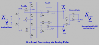
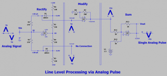
The attached is the complete schematic of this line level application to generate or synthesize an output Analog Signal which is [+H2]. The circuit is in three subunits which are separated by vertical line dividers.
1. The far left subunit is the precision rectifier which generates analog pulses.
2. The middle subunit modifies one analog pulse relative to the other via a controlled amplification.
3. The far right subunit use an OpAmp to sum the modified analog pulses and invert the reconstituted Output Analog Signal.
4. [+H2] is a symbol used by Mr. Pass. It denotes a positive phase second harmonic now entrained in this output analog signaL
5. This output signal shows that its positive-going component has a larger absolute amplitude than its negative-going component.
Here is my explanation of my brain's perception of say this 100 Hz frequency. What is its sonic value!
Drive a linear and non inverting power amp with this [+H2] output signal. This power amp then drives a boxed linear woofer.
The woofer cone moves forward to a certain distance by the positive-going component, and generates a certain sound pressure which pushes my ear drum inward.
The negative-going component of this signal which follows pulls in the box the linear woofer cone to a distance with a lesser incursion and thus a lower resultant sound pressure than during its forward motion. My brain says this sound is forward approaching; at me; because of this difference or unbalance in sound pressure from each component in the projected signal. My ear drum was pushed in further by the signal's positive going component and retractedc to a lesser extent by its negative going component.
Reverse the leads of the loudspeaker. The resultant projected sound is [-H2]. My ear drum is pushed in to a lesser distance than it is pulled ou .The 100 Hz note appears or is perceived to be receded in this [-H2] by comparison with my perception its forwardness in [+H2]. Mr. Pass has the best explanations for this.
Fastt Eddie D. The use of a vaccum tube is understood to imbibe its output signal with [H2]. It is a generator of this specific distortion as is the case here.
PRR. I believe the legitimate issue of crossover distortion which you raised lies primarily in the precision rectifier. Maybe further aggravated by time delays in the input stages of the OpAmps to follow. The net effect is the analog pulses are or may not be rejoined properly; saying this output signal was effectively processed in a Class B circuit.
Best wishes.
Anton
Attachments
Last edited:
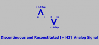
The attached picture depicts an alternative Output Analog Signal in/from the last post to explain PRR's concern. I thus corrupted it with crossover plus my intended [+H2] distortions. Please note:
1. The times t and t2 on the X axis mut be exactly superimposed [t2-t = 0] to endow this output signal fidelity and accuracy.
2. I understand that crossover distortion is best heard at low signals levels. Headphones can be a practical tool here to test. How many of us know to hear crossover distortion?
3. As shown, this signal is burdened with crossover and [+ H2] distortions. [+/-H2] are easy to hear. I have trained my hearing for [+/- H2] by using other independent Class A applications.
Best wishes
Anton.
Attachments
The objective of this second application is to create a single-ended amplifier. The style of this attached schematic is like the earlier ones. It has the following 3 sub-schematics.
1. Rectify [far left] which generates the output Analogs Pulses [AP} from the input Analog Signal [AS].
2. Modify the [APs] in the middle section. This shows that only the [AP] at times [t to t1] was amplified by a factor 2 The [AP] at times [0 to t] was not used.
3. Sum in the far right circuit the [AP] at times t to t1 of amplitude = +2Vp with a 1.5 V voltage from a battery.
4. The resultant output is a negative-going [AP] at times t to t1 riding on a fived voltage of -1.5 V.
The next post will show a simplified schematic of this line level processor. The post to follow will show the objective application.
Best wishes
Anton
Attachments
The attached is a simplified schematic of the precision rectifier processor I showed in the previous post.
The input Analog Signal [AS] passes through a set of OpAmps [U1]. The resultant output is a negative-going [AP] at times t to t1 riding on a fixed -1.5 V voltage. Note that the absolute peak amplitude of the output [AP] is two times that in/of the negative-going component in the input [AS].
Best wishes.
Anton
Attachments
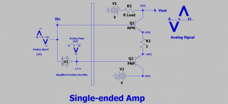
No reason to keep you in suspense; if any! The attached shows the schematic of this concept single-ended amp.
1. The simplified schematic of the precision rectifier processor in the previous post is to the left of the double-line vertical separator.
2. The "amplifier" circuit is to the rightside of this separator.
Notable is the BJT's are meant to idle at low current but do/will not cutoff at higher power levels.
I'll explain its works in the following post.
Best wishes
Anton
Attachments

While the whole scheme is very susceptible to lack of precision, the point I was making is that no matter how perfect the rectifier is, an instant change of gain at a point is a distortion. And perversely the more perfect the rectifier is the more it will stand out to the ear.PRR. I believe the legitimate issue of crossover distortion which you raised lies primarily in the precision rectifier.
A similar scheme is used in guitar effects to give an "octave up" sound, and only very im-perfect rectification works without harshness.
The change of gain across the audio wave should be s-p-r-e-a-d o-u-t over the whole wave.
Try it.
Thanks PRR for your insights and broader view of problems that can and/or plague already this approach of music amplification. I may further understand that objective rather than subjective measurements of signal fidelity are your principle concern. I do practice at home this general subject. Subjectively speaking, my perception of its music is like that of others.While the whole scheme is very susceptible to lack of precision, the point I was making is that no matter how perfect the rectifier is, an instant change of gain at a point is a distortion. And perversely the more perfect the rectifier is the more it will stand out to the ear.
A similar scheme is used in guitar effects to give an "octave up" sound, and only very im-perfect rectification works without harshness.
The change of gain across the audio wave should be s-p-r-e-a-d o-u-t over the whole wave.
Try it.
Please guide your suggestion above "try it" within the framework of this subject.
Best wishes
Anton
Here is this the operation of the single ended amp understudy. Please see the attached schematic. It is the same one I showed in the previous post.
1. The amplifier is [NPN +PNP]. It idles at a bias current = [1.5V -2 Vbe] divided by 1 ohm; which is the intra emitter's resistor [R2].
2. Let Vbe = 0.7 V. Thus the bias current flowing through both BJTs is [1.5 V - 1.4 V] divided by 1 ohm equals 100 mA.
3. The input Analog [music] Signal [AS] is simultaneously [in real time] presented to NPN and to the precision rectifier processor.
4. The positive-going component of [AS] enhances the conduction of NPN. PNP does not see an Analog Pulse during the same NPN enhancement time of [0 to t].
5. Let +Vp = 1V. Thus the resultant current flowing through either BJTs is ~1.1 A
6. The essence of this amp's operation follows below.
7.The negative-component of the music signal attempts to decrease the conduction of NPN.
8. PNP receives a simultaneous or a time coincident [t-t1] analog pulse having twice the absolute amplitude of that in the music signal.
9. At peak condition, the voltage drop across the intra emitter resistor [R2] is equal to [-2Vp -(-Vp) ] = -Vp = -1V.
10. This gives a negative-going signal current ~-1.1A. It has the same value as that from the positive-going component in the music signal.
11. The conduction of NPN stays enhanced during the full cycle of the input music signal. Ditto for PNP.
The load resistor to NPN can be a power output transformer, a lamp, a coil, a power resistor.
Best holiday wishes
Anton
Attachments
So you're saying a gradual transition with round edges will give a subjectively good effect? That makes sense.While the whole scheme is very susceptible to lack of precision, the point I was making is that no matter how perfect the rectifier is, an instant change of gain at a point is a distortion. And perversely the more perfect the rectifier is the more it will stand out to the ear.
A similar scheme is used in guitar effects to give an "octave up" sound, and only very im-perfect rectification works without harshness.
The change of gain across the audio wave should be s-p-r-e-a-d o-u-t over the whole wave.
Try it.
I've seen guitar distortion circuits that used back to back diodes in the feedback loop. It seems this would go hand in hand with compression.
As an aside, Chris Squire of Yes used distortion effects on his bass. He found that using a traditional "fuzz" effect also came with compression, which made the bass sound subjectively weak and lacking "punch." So he split the signal in two, and applied distortion effects only to the harmonics of the note. This preserved the "punch" and still added a euphonic effect to the bass.
EDIT: I mean parallel diodes.
I can't edit my post. I didn't think it was possible for me to hate the new forum more, but the more I use it the more frustrating it is.
I can't edit my post. I didn't think it was possible for me to hate the new forum more, but the more I use it the more frustrating it is.
Hello Fast Eddie D, and allEDIT: I mean parallel diodes.
I can't edit my post. I didn't think it was possible for me to hate the new forum more, but the more I use it the more frustrating it is.
I hope that your holidays continue to be pleasant and uneventful.
Thanks for your comments. Your post and maybe PRR's seem to suggest guitar applications; which have not crossed my mind. Pleaase attach a schematic for me to chew on, and to connect with this subject of processing via analog pulse.
Best wishes
Anton
- Home
- Source & Line
- Analog Line Level
- Analog Pulse Line Level