I finally got around to realize my class AB MOSFET amplifier but there are some mysterious problems.
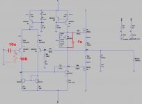
First of all I have the schematic in the pictures below, from my LTspice simulation. Many component values are in the parameters, beside the schematic. The output MOSFETS are the ECX10N20 / ECX10P20 from Exicon.
I also have adapted pictures of how the actual thing looks like. It is mounted on the heat-sink ready to go. And the long resistor snake is just a dummy 8Ω load that I calculated to be able to withstand around 100Watts.
The keen observer would distinguish that I am not using a linear PS, but a switch mode power supply, tailored for audio use. It is built by ConnexElectronic and I have its datasheet attached. The main takeaway is it is a +/-60V version, with a soft-start circuit and (most importantly for our problem) an overcurrent protection mechanism, that is triggered when the SMPS sees a short.
R4, R5 and Rsp2 in the schematic are all trimmers that I can adjust willingly to set the bias between the MOSFET gates at the proper value of 1,8V.
My first measurements were with the input grounded and without connecting a load (infinite load). I powered it and measured key voltages with my digital multimeter. Most of those voltages checked out just fine with the simulation, apart from the bias which was a bit lower than 1V, when it should be around 1,8V. I figured it is not a big problem since everything runs colder and it is safe for the time being. I could fix it later, playing with the trimmer values, after I have assessed that there is no bigger problem.
And now the trouble begins. I decided to connect my dummy load. At power-on everything is fine. I checked the transistors with my fingers to see if something is too hot and everything is ok. I checked supply voltages and they indeed were +/-60V. I checked the output node and the offset is something between 50mV to 100mV; not great, not terrible. And as soon as I touch even just one probe of my multimeter in the VAS node, the overcurrent protection is triggered and I immediately power everything off. I am quick to do that because the first time I was like ok I guess it will stop and I started checking the transistors with my finger and found that the P-channel MOSFET was starting to heat when overcurrent protection is triggered, along with the VAS transistor Q3, which is always a little bit hot, dissipating a power figure close to its maximum allowable one.
I seriously need to measure the bias voltage, which is the emitter-collector voltage of Q6. But I can't because the overcurrent protection is triggered. Milliseconds before it happened, I was able to measure the proper value of 1,8V between the gates though. And I conducted various tests, where I powered it on, and left it for a few minutes with the dummy load on. Nothing overheated, the protection didn't trigger and everything seemed fine, until I touched the VAS node again.
Please help my inexperienced, frustrated being...
Attachments
Are you operating the amplifier as shown in the simulation?
No decoupling capacitor or reference resistor on the input?
Dc offset would be incredible high. Around 100mv to 180mv
most likely negative. Im surprised you only have 60 to 100mv.
Bias is not set yet. With 100mv of DC offset. Likely negative voltage
would bias the p channel output mosfet very high.
DC offset needs to be corrected.
3 to 10 mv is acceptable.
60 to 100mv is not good at all
My suspicion is that the high capacitive load (or capacitive coupling to other parts of the circuit) of the multimeter/lead caused the amp to oscillate, probably at full power. Try adding a 10k series resistor to the probe so this capacitance isn't being seen directly.
Using a 'scope with x10 probe(s) is much more friendly to such a circuit under test than a multimeter, as this presents 10M in parallel
with a few pF and doesn't load down the node or radiate signal into space all around (multimeters act as loop antennas)
Using a 'scope with x10 probe(s) is much more friendly to such a circuit under test than a multimeter, as this presents 10M in parallel
with a few pF and doesn't load down the node or radiate signal into space all around (multimeters act as loop antennas)
I am indeed operating as shown in the simulation because I am making dc measurements. The input is grounded and thus I have used the small green jumper wire you see in the picture to connect the input to ground. The amplifier is just the power amp of a bigger guitar amplifier. The preceding stage has a decoupling cap and a reference resistor.Are you operating the amplifier as shown in the simulation?
No decoupling capacitor or reference resistor on the input?
Dc offset would be incredible high. Around 100mv to 180mv
most likely negative. Im surprised you only have 60 to 100mv.
Bias is not set yet. With 100mv of DC offset. Likely negative voltage
would bias the p channel output mosfet very high.
DC offset needs to be corrected.
3 to 10 mv is acceptable.
60 to 100mv is not good at all
As for the dc offset I tried my best without getting into too elaborate designs, but even the simulation it is around 50mV
I might make measurements with my oscilloscope then, using the x10 probes. i hope this goes smoothlyMy suspicion is that the high capacitive load (or capacitive coupling to other parts of the circuit) of the multimeter/lead caused the amp to oscillate, probably at full power. Try adding a 10k series resistor to the probe so this capacitance isn't being seen directly.
Using a 'scope with x10 probe(s) is much more friendly to such a circuit under test than a multimeter, as this presents 10M in parallel
with a few pF and doesn't load down the node or radiate signal into space all around (multimeters act as loop antennas)
i'm curious as why the 0v/gnd is on different connector then the +,- supply connections? i'm no expert on layout but doesn't that create a larger loop area making it more prone to noise and potential instability?
No DC decoupling. add a proper input network for testing.
then when you ground the input there wont be DC offset.
Also when driving mosfets directly from the vas, I have found amplifiers to be more stable
with 1 to 2.2u capacitor tied across the vbe transistor
then when you ground the input there wont be DC offset.
Also when driving mosfets directly from the vas, I have found amplifiers to be more stable
with 1 to 2.2u capacitor tied across the vbe transistor
Attachments
Last edited:
Solid advice. I will try adding a capacitor if oscillations persist. I think a small wima one will do. I will add an input network too, just for the testing.No DC decoupling. add a proper input network for testing.
then when you ground the input there wont be DC offset.
Also when driving mosfets directly from the vas, I have found amplifiers to be more stable
with 1 to 2.2u capacitor tied across the vas transistor
Haha you are absolutely right. It won't be like that when it is over though. It is just for dc measurements. You see the middle slot of the supply terminal is indeed ground but I used it to ground the input terminal. The terminal across the board next to the heatsink is just an aux ground for my tests. Inside the amp the signal ground will be mounted on the chasis, and I have a cable below the board that is the ground of the entire power amp, ready to go in the star grounding.i'm curious as why the 0v/gnd is on different connector then the +,- supply connections? i'm no expert on layout but doesn't that create a larger loop area making it more prone to noise and potential instability?
UPDATE:
Now I have another problem. I fixed the bias of the IPS to be around 2mA in the tail of the differential amp.
The VAS current was supposed to be around 10mA but that would mean that the VAS bjt would dissipate half a Watt, while its maximum allowable dissipation is around 0.6W. I expected it to get hot but it got too hot so I lowered the VAS current around 7,5mA to 8mA. It still gets hot but not as much
The problem now is that whatever I do with the trimmer Rsp2 of the bias spreader the bias between the gates is stuck at 0.6V, and I can't get it to more than 1V. Any idea what is going on?
I built an input network on my breadboard and the dc output problem got instantly better. I haven't added the capacitor yetNo DC decoupling. add a proper input network for testing.
then when you ground the input there wont be DC offset.
Also when driving mosfets directly from the vas, I have found amplifiers to be more stable
with 1 to 2.2u capacitor tied across the vbe transistor
I added 10k resistors on my meter and I was able to take proper measurements. Thanks!My suspicion is that the high capacitive load (or capacitive coupling to other parts of the circuit) of the multimeter/lead caused the amp to oscillate, probably at full power. Try adding a 10k series resistor to the probe so this capacitance isn't being seen directly.
Using a 'scope with x10 probe(s) is much more friendly to such a circuit under test than a multimeter, as this presents 10M in parallel
with a few pF and doesn't load down the node or radiate signal into space all around (multimeters act as loop antennas)
Now I have another problem. I fixed the bias of the IPS to be around 2mA in the tail of the differential amp.
The VAS current was supposed to be around 10mA but that would mean that the VAS bjt would dissipate half a Watt, while its maximum allowable dissipation is around 0.6W. I expected it to get hot but it got too hot so I lowered the VAS current around 7,5mA to 8mA. It still gets hot but not as much
The problem now is that whatever I do with the trimmer Rsp2 of the bias spreader the bias between the gates is stuck at 0.6V, and I can't get it to more than 1V. Any idea what is going on?
Those big white resistors are wire wound and have a lot of inductance, that alone can be enough to cause instability. Replace the ones on the pcb with low inductance types or place 100nf in parallel with each. For the dummy load this is not necessary
as soon as I added the capacitor (largest value I could find was 0.47u) the p-channel MOSFET started oscillating (overcurrent protection triggered and MOSFET getting hot). If I may rid myself of the source resistors things would be fineNo DC decoupling. add a proper input network for testing.
then when you ground the input there wont be DC offset.
Also when driving mosfets directly from the vas, I have found amplifiers to be more stable
with 1 to 2.2u capacitor tied across the vbe transistor
With latFETs you do not need source resistors!as soon as I added the capacitor (largest value I could find was 0.47u) the p-channel MOSFET started oscillating (overcurrent protection triggered and MOSFET getting hot). If I may rid myself of the source resistors things would be fine
The DC offset due to base current along the feedback resistor should have shown up in the simulation.No DC decoupling. add a proper input network for testing.
then when you ground the input there wont be DC offset.
Also when driving mosfets directly from the vas, I have found amplifiers to be more stable
with 1 to 2.2u capacitor tied across the vbe transistor
No input biasing resistor. No input coupling capacitor.
No input RF filter.
Cm should be around 47 to 100pf.
Get rid of source resistors.
You can use a simple pot for Vbe multiplier for lateral mosfets.
See Maplin lat mosfet circuit for examples. 27pf's were a bit small and some ocillated otherwise worked well.

No input RF filter.
Cm should be around 47 to 100pf.
Get rid of source resistors.
You can use a simple pot for Vbe multiplier for lateral mosfets.
See Maplin lat mosfet circuit for examples. 27pf's were a bit small and some ocillated otherwise worked well.
You don't need that much current to drive MOSFETs, the gate charge is measured in nanocoulombs, and the gates swing perhaps 6 to 8V peak, so 1mA drive is probably enough for 20kHz - 2mA in the VAS ought to handle that.The VAS current was supposed to be around 10mA but that would mean that the VAS bjt would dissipate half a Watt, while its maximum allowable dissipation is around 0.6W. I expected it to get hot but it got too hot so I lowered the VAS current around 7,5mA to 8mA. It still gets hot but not as much
The Exicon devices allegedly have protection built-in, but I can't seem to find chapter&verse on this and would add back-to-back protection zeners (or a TVS diode) between gate and source with knee around 10V.
Correct, Op states his simulation shows 50 mv DC offset.The DC offset due to base current along the feedback resistor should have shown up in the simulation.
Real world measurements show 60 to 100 mv
I didnt need to simulate the amplifier to already know that would happen.
But did simulation to see why P channel mosfet is unstable.
My simulation shows exact same results as real world measurements, and assumed behavior.
100 mv of DC offset on output, DC offset causes p channel to Bias 40 mv higher.
P channel Mosfet is unstable in simulation.
I got the amplifier to be more stable by reducing LTP degeneration from 100 to 22 ohms.
Reduced Vas current to 4 ma.
Removed Mosfet source resistors.
High frequency performance would be horrible with 220p Vas compensation. reduced to 33p
With proper input DC decoupling on input, DC offset is .3 to 2mv depending on current source temperatures
Overall Gain of amplifier is very low, close to 3volts needed for full power.
Likely not a issue since I believe its for Musical Instrument use, and might have high gain pre amp.
Hitachi/Maplin amplifier shown in post #15 is good suggestion. Believe Maplin sold it as guitar kit
common mod is to remove R3 47k resistor and replace with 1 to 2ma Current source
Last edited:
UPDATE
Now I have another problem (problems are never ending it seems). And it is the SMPS. God it's noisy... I mean I get huuuge interference in the output. Pretty logical as I used zero supply filtering. I have a filtering network as you see in my photos but I disconnected it because I thought it was causing problems in some earlier design stage. Turns out it wasn't. Anyway I am adding it back now. This thing is so noisy that I am thinking of soldering a small 0,1uF cap directly in the drain pins of each mosfet to a close ground node I have, apart from the network of bigger caps I have. Do you think this is a good practice?
Thanks for the thorough work my friend! I worked out some of the things you did myself. I got rid of the source resistors and everything stabilized. I also lowered the VAS current to around 6mA but I might lower it some more. The Miller cap is such a high value because the gain margin is small and I don't care about high slew rates and good hf frequency performance. This is for a guitar amp so everything above 5kHz is being attenuated more or less. I added a proper input network with an RF filter that has a very low cut-off frequency of 23kHz because, again, this is a guitar amp. The low gain is also due to it being a guitar amp as you guessed and also a small one. The output offset is now super low, something like 10mV which is awesome.Correct, Op states his simulation shows 50 mv DC offset.
Real world measurements show 60 to 100 mv
I didnt need to simulate the amplifier to already know that would happen.
But did simulation to see why P channel mosfet is unstable.
My simulation shows exact same results as real world measurements, and assumed behavior.
100 mv of DC offset on output, DC offset causes p channel to Bias 40 mv higher.
P channel Mosfet is unstable in simulation.
I got the amplifier to be more stable by reducing LTP degeneration from 100 to 22 ohms.
Reduced Vas current to 4 ma.
Removed Mosfet source resistors.
High frequency performance would be horrible with 220p Vas compensation. reduced to 33p
With proper input DC decoupling on input, DC offset is .3 to 2mv depending on current source temperatures
Overall Gain of amplifier is very low, close to 3volts needed for full power.
Likely not a issue since I believe its for Musical Instrument use, and might have high gain pre amp.
Hitachi/Maplin amplifier shown in post #15 is good suggestion. Believe Maplin sold it as guitar kit
common mod is to remove R3 47k resistor and replace with 1 to 2ma Current source
Now I have another problem (problems are never ending it seems). And it is the SMPS. God it's noisy... I mean I get huuuge interference in the output. Pretty logical as I used zero supply filtering. I have a filtering network as you see in my photos but I disconnected it because I thought it was causing problems in some earlier design stage. Turns out it wasn't. Anyway I am adding it back now. This thing is so noisy that I am thinking of soldering a small 0,1uF cap directly in the drain pins of each mosfet to a close ground node I have, apart from the network of bigger caps I have. Do you think this is a good practice?
maybe i missed it - what values resistors are you using in series with the mosfet gates?
for this type of construction, it makes a significant difference.
And do you have a scope that can give you some idea of the frequency of oscillations to confirm it is the MOSFETs?
for this type of construction, it makes a significant difference.
And do you have a scope that can give you some idea of the frequency of oscillations to confirm it is the MOSFETs?
- Home
- Amplifiers
- Solid State
- DC measurements problems on original MOSFET class AB design