Hi
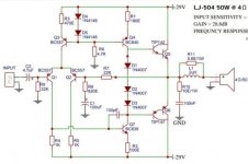
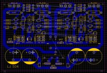
I am trying to make a PCB layout for the Amplifier circuit given below. As it's my first attempt in PCB design I need your suggestions and corrections for the layout. I made this with EasyEda .
This circuit was created in a local amplifier designing workshop done by Mr. Joshy Liadel.
Will it have some issue if a power supply section is included in the amplifier PCB.
Attachments

was this design created strictly for pcb layout practice or is the intent to have a correctly working and fully operational amplifier afterwards?
is this a tested design?
is this a tested design?
There was a session by Mr Joshi on how to design an amplifier . Right from block diagram to final schematics ,calculations and selection of components this circuit was designed in that excercise. He has given permission for all to use this circuit . The circuit is alredy tested by many participants and got good results . Some of the participants who are in this business has already started selling this Amplifier . Pcb layout was not discussed there , so I thought of doing one and made the above layout . As I don't jave any knowledge about pcb layout I have posted it here for suggestions .
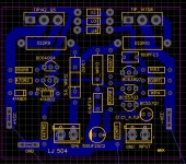
Most of my comments are about the silk screen layer:
1: Do not put writing under components, hard to read once the part is in place
2: Do not put values only part numbers in the print. Part values often change
3: Face all polarized parts (diodes, capacitors, transistors etc.) in the same direction. This makes assembly and trouble shooting much easier
4: C1 is shown twice, one as a 4.8uF
5: Do not use angles <90 deg. on traces and make traces as short as possible
Be creative and have fun! E
I'd probably move the power FASTON connectors to the other end of the PCB so they are close to the output transistors. The grounding needs a bit of work. Separate the quiet input ground from the high current speaker ground. I'd also include a position for one extra diode in the chain D1,D2, D3, just in case you need it. The junction of the emitter resistors; you really want to keep both sides of this track the same length and position the output components centrally. C1 needs to be bipolar, not polar. Larger the better. The 4u7 input coupling capacitor should probably be changed to something larger, 10-47uF for best LF response.
(1)Hi
I am trying to make a PCB layout for the Amplifier circuit given below. As it's my first attempt in PCB design I need your suggestions and corrections for the layout. I made this with EasyEda .
This circuit was created in a local amplifier designing workshop done by Mr. Joshy Liadel.
Will it have some issue if a power supply section is included in the amplifier PCB.
The pickup point for feedback isn't from the speaker terminal, so it will see IR voltages in the traces between the pickup point and the speaker terminal, voltages that are distorted half-waveforms.
For instance even if the trace has only 5 milliohms and the load is 8 ohms you are injecting upto 0.06% of the half-waveform which is about 0.03% distortion products.
I'd run a thin trace from just below the inductor pad, not from halfway between that and the emitter resistor. Then the feedback network sees no half-waveform IR contributions, just the actual voltage going to the speaker.
(2)
You might want decoupling on the rails, 50 to 100uF or so, and reverse diodes between rails and output to prevent reactive loads driving the output beyond the rails.
The bulk capacitance in the power supply is often too far away (in terms of inductance) to act as efficient decoupling for the amp pcb, risking full power oscillation of the amp - local decoupling prevents this.
(3)
You have no RF filter on the input - 100pF to 0.5nF or so to ground on the input terminal may be useful to help prevent RF pickup, especially with a BJT input section.
(4)
No thermal compensation. It will likely undergo thermal runaway.
Make it two layer.
Aside from the obvious ability to cross tracks that this gives, the production process for two layer boards provides plated holes, that are much, much more reliable when soldered.
Aside from the obvious ability to cross tracks that this gives, the production process for two layer boards provides plated holes, that are much, much more reliable when soldered.
Excellent suggestions above.
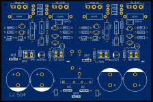
I´d add that as shown input and output wires exit towards main supply caps, which is clumsy, try to move them to a better place as suggested above or at least rotate them 90 degrees so wires exit sideways, into "free" space.
Filter caps are large and tall and in the way.
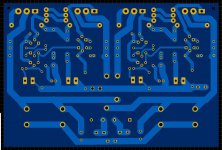
Your last picture seems to show a Ton of still unconnected pads, you still have a lot of work ahead to solve those paths.
It´s acceptable to need a couple jumpers if that avoids going double face, and short jumpers at that, but you are showing over 20 of them, criscrossing all over the board.
You are on the good path, but keep perfecting that board.
Congratulations.
I´d add that as shown input and output wires exit towards main supply caps, which is clumsy, try to move them to a better place as suggested above or at least rotate them 90 degrees so wires exit sideways, into "free" space.
Filter caps are large and tall and in the way.
Your last picture seems to show a Ton of still unconnected pads, you still have a lot of work ahead to solve those paths.
It´s acceptable to need a couple jumpers if that avoids going double face, and short jumpers at that, but you are showing over 20 of them, criscrossing all over the board.
You are on the good path, but keep perfecting that board.
Congratulations.
Component layout and placement on the board is key to good, direct routing.
If the schematic is well drawn, the layout should follow it as much as possible,
unless the board size must be minimized.
If the schematic is well drawn, the layout should follow it as much as possible,
unless the board size must be minimized.
Thank you all for the excellent suggestions, since I am totally new to this could you please elaborate some points .
Could you please tell bit more about the pickup point positioning?
The designer of this amp told to place the diodes on the same heat sink as output transistors, is that thermal compensation being referred to?
Do i have to totally isolate them or move them apart ?. Separate the quiet input ground from the high current speaker ground .
(1)
The pickup point for feedback isn't from the speaker terminal, so it will see IR voltages in the traces between the pickup point and the speaker terminal, voltages that are distorted half-waveforms.
For instance even if the trace has only 5 milliohms and the load is 8 ohms you are injecting upto 0.06% of the half-waveform which is about 0.03% distortion products.
I'd run a thin trace from just below the inductor pad, not from halfway between that and the emitter resistor. Then the feedback network sees no half-waveform IR contributions, just the actual voltage going to the speaker.
(4)
No thermal compensation. It will likely undergo thermal runaway.
Could you please tell bit more about the pickup point positioning?
The designer of this amp told to place the diodes on the same heat sink as output transistors, is that thermal compensation being referred to?
Give the circuit diagram to a PCB maker, they have software that makes all this a lot easier.
They have libraries for parts and so on. They will do a far better job, it is automatic in the software.
So for them it is a routine job.
If you are in Kerala, Bangalore, Mumbai and Chennai people might be easier, I use a local PCB maker. He will take at most half an hour, and try to avoid common errors like too many jumpers, and bad layout.
Last edited:
It is a pretty ordinary TIP 42/47 circuit with BC557 in input, what is so great about it?
You can find all of the details on line. PCB screens, and all.
You can find all of the details on line. PCB screens, and all.
Give the circuit diagram to a PCB maker, they have software that makes all this a lot easier.
They have libraries for parts and so on. They will do a far better job, it is automatic in the software.
So for them, it is a routine job.
If you are in Kerala, Bangalore, Mumbai, and Chennai people might be easier, I use a local PCB maker. He will take at most half an hour, and try to avoid common errors like too many jumpers and bad layout.
Dear NareshBrd,
That can be done very easily, I could get designed and delivered in a day. Already some versions of PCBs for this circuit are available, I could just buy it and save lots of time and effort. But my intention is to learn more about PCB layout that's why I posted this here.
Last edited:
Read one year of Elektor and other hobby magazines.
You will learn much more than what you will with this project about PCB design.
And if it is automated, why do you want to learn?
Concentrate on circuit design.
This circuit is about 30 years old, even the original transistors are hard to get.
Stop wasting everybody's time, be creative, do something new and different.
All this effort for a one off item that has been buried for years....
Last edited:
I have not asked for any circuit suggestions or advice on what things I have to learn or not. I never claimed that this is a great circuit. And I have not forced anyone to spend their time on the topic I posted. If you want to contribute to the design part please continue or you can ignore this thread.
Can this Amplifier use +36 0 -36 power supply ? If so, what changes should be made ?Hi
I am trying to make a PCB layout for the Amplifier circuit given below. As it's my first attempt in PCB design I need your suggestions and corrections for the layout. I made this with EasyEda .
This circuit was created in a local amplifier designing workshop done by Mr. Joshy Liadel.
Will it have some issue if a power supply section is included in the amplifier PCB.
You are completely missing the EDUCATIONAL side of this project.Give the circuit diagram to a PCB maker, they have software that makes all this a lot easier.
They have libraries for parts and so on. They will do a far better job, it is automatic in the software.
So for them it is a routine job.
If you are in Kerala, Bangalore, Mumbai and Chennai people might be easier, I use a local PCB maker. He will take at most half an hour, and try to avoid common errors like too many jumpers, and bad layout.
Now you are dissing the designer and his teacher.It is a pretty ordinary TIP 42/47 circuit with BC557 in input, what is so great about it?
You can find all of the details on line. PCB screens, and all.
What part of SCHOOL PROJECT you do not understand?This circuit was created in a local amplifier designing workshop done by Mr. Joshy Liadel.
Can YOU design a better one?
Please show us.
Congratulations.But my intention is to learn more about PCB design that's why I posted this here.
REALLY????? 😱Give the circuit diagram to a PCB maker, they have software that makes all this a lot easier.
They have libraries for parts and so on.
DOING beats "reading" 1000:1Read one year of Elektor and other hobby magazines.
You will learn much more than what you will with this project about PCB design.
Why learn and do anything if everything can be bought in Alibaba?And if it is automated, why do you want to learn?
Classroom examples still suggest 741 and 2N2222, guess why?Concentrate on circuit design.
This circuit is about 30 years old, even the original transistors are hard to get.
Does generic/classic/basic ring a bell?
ANYTHING done for the first time is new and different.Stop wasting everybody's time, be creative, do something new and different.
In a magazine? .... maybe.All this effort for a one off item that has been buried for years....
You are missing this project has been freshly designed, using all the Math necessary, from the ground up, at a Classroom, a couple Months ago.
I suggest you never ever learn to play the guitar, what for?
After a few classes you will NOT play like Paco de Lucia or Yngwie Malmsteen, so, why bother?
Better listen to Spotify.
TIP 41B good to 80V
TIP41C good to 100V.
JMF, you do not know how things work in India, the project is needed in final year engineering (degree), or you can't give the exam.
The external examiner should not come to know you copied somebody else's work.
Problem is we have about 200,000 engineering graduates finishing each year, and it is group of 4, so 50,000 unique projects must be done each year.
Kind of difficult.
So an old obscure circuit is chosen...TIP41 is ancient.
Most graduate electronics engineers here cannot solder properly.
Hardly any mechanical engineers know how to use a timing light on a car, if they even know what it is.
My father is a graduate civil engineer, he had a complaint from a colleague, what to do about this joker?
The joker was a graduate electrical engineer trying to check the input to the cathodic protection transformer with an ordinary incandescent bulb.
(Step down transformer, supply to rectifier, that was used for cathodic protection of cross country oil pipelines).
Problem was it was 11kV, luckily the supply was shut off from the outside.
He was from a special tribe, they get admission and jobs at 40%, and are difficult to fire.
We ordinary people are lucky to get college seats at 90% high school exam results.
He was transferred to a desk job, with a remark in his confidential report that he never be posted in the field.
Must have retired now.
Think what happens when you touch 11kV with a wire insulation rated for 600V.
So, if I tell somebody from my country what to do, please bear in mind that I am local.
I am aware of their level of competence.
Last edited:
WHERE does the OP say that this is an Engineering Degree final project?
On the contrary, he clearly states it´s a "first design carried out in a classroom", where the Teacher is Mr Joshy Liadel .
Guess we are talking High School level here and it´s quite appropriate there.
It might even be an extra curricular project, carried out at some City Youth center or similar, to get Youth interested into something useful, outside of the streets, and getting proficient on something besides Tik Tok binge watching, endless Whatsapp chatting or gaming.
You´d be surprised at how SIMILAR India and Argentina are in many important aspects. 😉
- Home
- Amplifiers
- Solid State
- Need help in Amplifier PCB layout