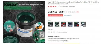
Hi, about this solder mask (attached)
Most of the videos showing application use transparent plastic film as a layer, between the solder mask and the printed layout.
But there are problems after UV curing - taking the plastic film off could cause the solder mask to be removed from the PCB.
I have similar problems with dry photoresist film - sometimes it peels of the pcb.
Is there any agent, than can cause the applied on pcb solder mask to become dry?
So that it is stuck to the pcb and exposed without the extra transparent film.
Attachments
WHICH one are you using?Hi, about this solder mask (attached)
Most of the videos showing application use transparent plastic film as a layer, between the solder mask and the printed layout.
But there are problems after UV curing - taking the plastic film off could cause the solder mask to be removed from the PCB.
I have similar problems with dry photoresist film - sometimes it peels of the pcb.
Is there any agent, than can cause the applied on pcb solder mask to become dry?
So that it is stuck to the pcb and exposed without the extra transparent film.
You write about dry film, the picture shows paint type one, which is applied by silkscreening, completely different.
Doubt dry films became too dry, I much suspect your PCB surface is drirty/greasy/contaminated (you must NOT touch it with bare hands) OR you are not applying the proper application technique.
I always silkscreen "everything", because I work commercially and make batches of any PCB, and liquid ink wets surfaces very well, not sure (never used) how you activate dry film to make it stick.
Solvent to make it tacky? Heat and pressure? Self adhesive like Scotch tape?
Again: suspect more PCB surface condition than anything else.
Ordering PCBs in China is not really solving the problem, just paying somebody else to do it right, not the same thing 🙂
I always silkscreen "everything", because I work commercially and make batches of any PCB, and liquid ink wets surfaces very well, not sure (never used) how you activate dry film to make it stick.
I do mostly the same as you do. But as I'm a cheap bastard, I use masking tape and the little dot stickers you can get from the office store to mask the areas I don't want the layer on 😱
You love handwork then 🙂
For prototypes I keep it very simple: no solder mask which is a luxury and instead I spray shiny clean copper surface with blue or red or green dyed pine-rosin-in-alcohol solution, board then *looks* very much like a solder masked one, of course hot solder melts it and solder "takes" on pads, not solder resist but actually solder help he he.
We are talking early prototype stages where important changes and editing are still much expected.
When it´s "set in stone" (sort of, Murphy´s Law always applies) then a proper 2 component Epoxy solder resist layer is screened.
No UV curing but plain old Epoxy chemical hardening.
VERY trusty and repeatable.
And actually faster, if making a batch, about 30 seconds (or less) per print.
The ANNOYING part is PERFECTLY cleaning the Schablon, once Epoxy hardens, even if atoms left behind, it stays on the silk forever, clogging small detail.
Oh well.
Usually jars of solder mask are intended for touch-up following repair if you somehow managed to damage the solder mask.
Tom
Tom
- Home
- Design & Build
- Equipment & Tools
- chinese UV solder mask drying