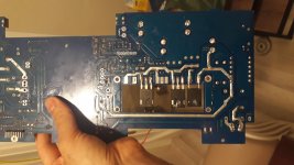
All straight tracks, so KiCad could be used to duplicate that board.
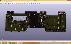
Just a simple two layer with a big cut out.
The tinned tracks shows that it had current problems, so 2oz copper would be a good idea.
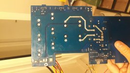
Just a simple two layer with a big cut out.
The tinned tracks shows that it had current problems, so 2oz copper would be a good idea.
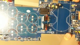
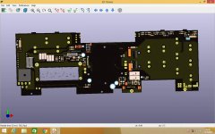
The tinned tracks shows that it had current problems
Not really. It's just a way of beefing up the current carrying capacity of the trace. That doesn't indicate a problem. One could also just make the traces wider.
The odd thing is that the tinned traces are actually on top of pours in most places. That's a really bizarre choice.
If the tinning is what OP is looking to recreate, all that's needed is to draw a line on the solder mask layer where you want the tin to be. That creates an opening with the solder mask where you can apply the solder. In a professional assembly flow, the tin is picked up during wave soldering.
Tom
Last edited:


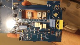
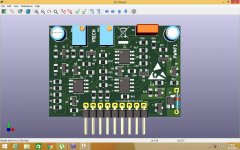
KiCad would allow you to make a composite pad like that by placing several THT pads together with the same pin number.
I would avoid copying this exactly and use regular vias nearby to stitch the layers for more current capacity, as those holes look to be too close to the drilling limits. PCB fabs hate breaking drill bits when the hole breaks out.
I would avoid copying this exactly and use regular vias nearby to stitch the layers for more current capacity, as those holes look to be too close to the drilling limits. PCB fabs hate breaking drill bits when the hole breaks out.

Kicad
Kicad is great thanks all
Kicad is great thanks all
Attachments
Last edited:
- Home
- Design & Build
- Software Tools
- which pcb program can do it ?