I am hoping to get some help with my First Watt B1 buffer preamp build. I noticed a subtle distortion that is more apparent at lower frequencies when plugged into First Watt J2 amp.
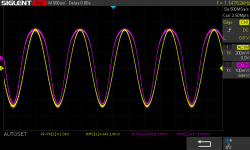
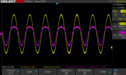
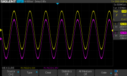
Bench test (B1 alone) is with a 1kHz sine wave at 1V. Power supply for preamp is a 24V wall wart. The findings are identical on both channels. The yellow trace is input, purple is output across a 100k Ohm load.
My questions:
1) The top part of the output wave is wider than the input signal. Is this the source of the audible distortion and can you suggest a cause or systematic approach to fix it?
2) The B1 has no voltage gain as designed, but should there be “voltage loss”? The output voltage is about half of the input.
Any help is greatly appreciated. Many thanks.
Rich
Attachments
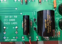
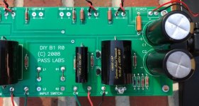
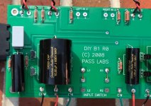
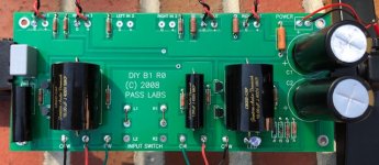
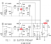
Is this the original B1 with 2 - 2SK170 per channel?
If yes, are the 2SK170s matched?
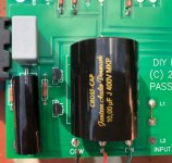
Clear, focused pictures please.
Was the volume pot at maximum volume during test?
Yes, the output waveform is distorted.
If yes, are the 2SK170s matched?
Clear, focused pictures please.
Was the volume pot at maximum volume during test?
Yes, the output waveform is distorted.
Well, the output is not necessarily wider - you moved the 0V line up about half the signal height (64mV) - can you maybe rather set both channels to the same resolution and the Y offset to both 0V? It looks more like the positive half of your signal is cut off.
your signal is clipping. And since you report you loose halve of the input amplitude, it make we wonder if you are loading with 100R instead of 100kOhm
Is this the original B1 with 2 - 2SK170 per channel?
If yes, are the 2SK170s matched?
Yes, purchased from passdiy.com.
Clear, focused pictures please.
attached
Was the volume pot at maximum volume during test?
yes
Well, the output is not necessarily wider - you moved the 0V line up about half the signal height (64mV) - can you maybe rather set both channels to the same resolution and the Y offset to both 0V?
attached
It looks more like the positive half of your signal is cut off.
I think you are right.
your signal is clipping. And since you report you loose halve of the input amplitude, it make we wonder if you are loading with 100R instead of 100kOhm
I double checked. Load is 100kOhm.
Attachments
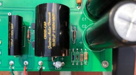
23.9V is not good. It should be approximately 12V.
Check the solder joints, especially around JFETs.
Joints look ok. Any chance transistors are backwards with respect to source and drain??
What is the voltage drop across R1?
0.02V
Also voltage at these two points relative to Ground?
22V @ gate of Q100 and Q200
Also, are both R2 and R3 10k (or, at least of equal resistance)?
Yes, confirmed.
I am very appreciative of your patience and assistance in troubleshooting. Thank you! Rich
R2 is measuring 24V with respect to ground on both sides. I believe this is a voltage dividing circuit and the "lower part" of R2 should measure 12V, not 24V. Am I thinking about this correctly and could that indicate a bad resistor?
The distortion is equal and identical in both channels which leads me to think it's a power supply issue. What do you think??
The distortion is equal and identical in both channels which leads me to think it's a power supply issue. What do you think??
Or bad D1?
The 0.02V across R1 is good, indicating that the CCSs are working.
So bad resistor or diode?
The 0.02V across R1 is good, indicating that the CCSs are working.
So bad resistor or diode?
Or bad D1?
The 0.02V across R1 is good, indicating that the CCSs are working.
So bad resistor or diode?
I'm showing my inexperience here- what is CCS?? Thx
Constant Current Source Q101 and Q201 with their gate tied to ground. The schematic calls for 18v, you are using 24v, have you tried 18v? Get a 7818 voltage regulator and you can make one easily enough.
Or if you have a bunch of 1N400x diodes lying around, string 10 in series and put between your wall wart and the board. You will get (10x 0.6v) 6v of drop and about 18v to check if your circuit works.
Or if you have a bunch of 1N400x diodes lying around, string 10 in series and put between your wall wart and the board. You will get (10x 0.6v) 6v of drop and about 18v to check if your circuit works.
Last edited:
Rich,
Here is some information:
PassDiy
"The buffer uses an external power supply from 18 to 24 Volts DC. You can power it with batteries, but most convenient is an external regulated supply running off the wall. The preamp typically draws fewer that 0.02 Amps, so current is not much of an issue. A regulated supply is better, but the circuit is pretty good at ignoring noise on the supply and minor fluctuations."
Also:
"Q101 and Q201 are constant current sources formed by simply attaching the Gate pins of the JFETs to the Drain pins. They provide without loading them down or creating significant distortion."
The 0.02V across R1, which is 1 Ohm, indicates 0.02V/1 Ohm=0.02A, which is as designed. So the CCS (Q101 and Q201) are working.
As mentioned by Mr. Pass, 24V supply is acceptable.
Have you looked into D1? Right now the voltages at their gates and sources of Q100 and Q200 are problematic.
Ben,
I removed D1 and the waveform looks perfect!
One last question- why did you think it was D1 rather than one of the voltage divider resistors?
Thanks a million for your help!
Rich
I removed D1 and the waveform looks perfect!
One last question- why did you think it was D1 rather than one of the voltage divider resistors?
Thanks a million for your help!
Rich
Attachments
Last edited:
Well, if R3 or C2 was shorted, then V=0. If R2 or D1 was shorted, then V=24V. Usually resistors do not short easily but small diodes can be damaged with too much heat.
You can test the diode with your multimeter.
It's great that the B1 is now working properly.
You can test the diode with your multimeter.
It's great that the B1 is now working properly.
- Home
- Amplifiers
- Pass Labs
- B1 Buffer Preamp Distortion