About the rare failure of the output inductor,Worse distortion performance,need help~
About the rare failure of the output inductor, why does it significantly worsen the distortion data? I need help~
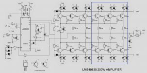
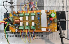
In order to verify whether the circuit is normal, I built a test circuit board. There are only a few differences between the test circuit board and the circuit diagram. The test board eliminates the power tube in the blue box, and the current amplifier stage uses only two pairs of NJW0302/0281. The rest is exactly the same.
I tried to reduce the gain to 26dB to optimize the distortion performance as much as possible, and reduce the value of the negative feedback resistor to optimize the noise performance as much as possible. After testing, this is the best performance that the temporary test circuit board can achieve:
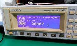
THD+N (8Ω/50W and 80kHz bandwidth):
20Hz 0.0009%
1kHz 0.0007%
20Khz 0.0017%
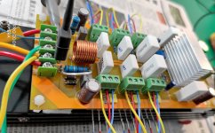
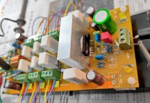
But in the experiment I encountered a strange problem. The output inductor on the test board will seriously deteriorate the distortion performance. When using a 3uH vertically placed output inductor, 20Khz THD+N 0.01%! When using 1uH horizontally placed output inductor, 20KhzTHD+N 0.007%! When I short-circuit the output inductor with a piece of wire, THD+N has been amazingly improved~It's unbelievable...
I have checked the square wave step response of the amplifier with a 100Mhz oscilloscope. There is no obvious overshoot or damped oscillation. No obvious parasitic oscillation was found on the sine wave.
I checked the materials of the two inductors and I confirmed that they are copper.
I checked the Zobel resistor and confirmed that it is not damaged.
The power transformer is placed far away, it should not cause electromagnetic interference, and I have tried to change the orientation of the test circuit board, but it has no effect.
I can't find the cause of the problem~~
Friends, can anyone tell me how to solve this problem? What caused it?
thank you all
About the rare failure of the output inductor, why does it significantly worsen the distortion data? I need help~
In order to verify whether the circuit is normal, I built a test circuit board. There are only a few differences between the test circuit board and the circuit diagram. The test board eliminates the power tube in the blue box, and the current amplifier stage uses only two pairs of NJW0302/0281. The rest is exactly the same.
I tried to reduce the gain to 26dB to optimize the distortion performance as much as possible, and reduce the value of the negative feedback resistor to optimize the noise performance as much as possible. After testing, this is the best performance that the temporary test circuit board can achieve:
THD+N (8Ω/50W and 80kHz bandwidth):
20Hz 0.0009%
1kHz 0.0007%
20Khz 0.0017%
But in the experiment I encountered a strange problem. The output inductor on the test board will seriously deteriorate the distortion performance. When using a 3uH vertically placed output inductor, 20Khz THD+N 0.01%! When using 1uH horizontally placed output inductor, 20KhzTHD+N 0.007%! When I short-circuit the output inductor with a piece of wire, THD+N has been amazingly improved~It's unbelievable...
I have checked the square wave step response of the amplifier with a 100Mhz oscilloscope. There is no obvious overshoot or damped oscillation. No obvious parasitic oscillation was found on the sine wave.
I checked the materials of the two inductors and I confirmed that they are copper.
I checked the Zobel resistor and confirmed that it is not damaged.
The power transformer is placed far away, it should not cause electromagnetic interference, and I have tried to change the orientation of the test circuit board, but it has no effect.
I can't find the cause of the problem~~
Friends, can anyone tell me how to solve this problem? What caused it?
thank you all
Attachments

wrong place for output coil. enclosed by power supply rails. place the coil outside the loop. (outside the pcb)
The output zobel should be after the inductor/resistor and as close to the speaker terminals as possible.
All those CE wire pairs to the output devices will be radiating harmonics to the inductor. Try twisting the Collector and Emitter wires together for each OP transistor
At such levels of distortion and load currents, the length and thickness of the printed conductors, their relative position, the position of the exit point and the gnfb point may matter.
49830 usually works with several pairs of mosfets. You intend to use 6 single BJT connected in parallel. The opposite effect of the load on the driver is possible.
49830 usually works with several pairs of mosfets. You intend to use 6 single BJT connected in parallel. The opposite effect of the load on the driver is possible.
Last edited:
best to avoid the output coil (when the desired distortion is less than 0.001%) . make a stable amplifier with only 0.1uH output inductor (approx. 30cm wire from PCB to output terminal)
https://www.eeweb.com/tools/parallel-wire-inductance/
https://www.eeweb.com/tools/parallel-wire-inductance/
Last edited:
This problem is discussed in detail in Self's book:
Audio Power Amplifier Design: Amazon.co.uk: Self, Douglas: 9780240526133: Books
Audio Power Amplifier Design: Amazon.co.uk: Self, Douglas: 9780240526133: Books
Not sure if this could be a reply. Try to glue the coil turns so the turns do not move when load current is flowing through it. I have seen coil turns repel and attract each other under heavy current in industrial applications and has to be sealed in some sort to prevent any movement. Regards.
Part LME49830At such levels of distortion and load currents, the length and thickness of the printed conductors, their relative position, the position of the exit point and the gnfb point may matter.
49830 usually works with several pairs of mosfets. You intend to use 6 single BJT connected in parallel. The opposite effect of the load on the driver is possible.
Description Mono High Fidelity 200 Volt MOSFET Power Amplifier Input Stage.
Maximum Output Current Current from Output pins 56 47 mA (min)
You seriously decided to replace the mosfet with single BJT and not darlingtons?
LME49830 Stage Datasheet pdf - Input Stage. Equivalent, Catalog
In your circuit, the IC is overloaded in output current. Output affects performance degradation.
Last edited:
Great suggestion, thank you!All those CE wire pairs to the output devices will be radiating harmonics to the inductor. Try twisting the Collector and Emitter wires together for each OP transistor
The good news is that the official version of the circuit board should not have this problem😀
I think Zobel provides a stable load for the amplifier at high frequencies. The zobel close to the amplifier will help stabilize the circuit. In fact, many circuit diagrams also place the zobel in front of the output inductor. There is a lot of debate about where the zobel should be placed. Are there any credible conclusions? thank you!The output zobel should be after the inductor/resistor and as close to the speaker terminals as possible.
At such levels of distortion and load currents, the length and thickness of the printed conductors, their relative position, the position of the exit point and the gnfb point may matter.
49830 usually works with several pairs of mosfets. You intend to use 6 single BJT connected in parallel. The opposite effect of the load on the driver is possible.
Yes, I think my test circuit board needs to be optimized. There are many things that can be improved in some details such as wiring layout. Negative feedback sampling point I adopted Self Douglas's suggestion, there should be no problem.
Although the LME49830 is designed to drive FETs, it is not mentioned in the technical manual that it cannot be used to drive BJTs. On the contrary, the manual mentions driving BJT, although there is only one sentence: "Pay attention to temperature compensation". The biggest difference between LME49830 and LME49810 is that 49810 uses traditional emitter-following circuit output, while 49830 uses totem pole circuit output. The latter is more conducive to driving FETs, but it does not seem to have any obvious adverse effects when driving BJTs. As you can see, when the output inductor is not used, it works quite well.
In addition, the LME49830 does not directly drive 6 pairs of BJTs. The actual structure is that 1 pair of BJTs act as a driver stage to drive 5 pairs of BJTs in parallel.This is a 3-level FE output stage. The two-level NJW0302/0281 can provide 10,000 times current amplification capability without overloading the IC.
thank you very much🙂
Yes, I have read his book seriously, his book is very good!This problem is discussed in detail in Self's book:
Audio Power Amplifier Design: Amazon.co.uk: Self, Douglas: 9780240526133: Books
The book mentions the crosstalk and induced distortion of the output inductor, I just thought that this part of the impact may not be too serious, I underestimated its impact! thank you!
Very good suggestion! I should indeed fix itNot sure if this could be a reply. Try to glue the coil turns so the turns do not move when load current is flowing through it. I have seen coil turns repel and attract each other under heavy current in industrial applications and has to be sealed in some sort to prevent any movement. Regards.
Thank you
wrong place for output coil. enclosed by power supply rails. place the coil outside the loop. (outside the pcb)
Very good suggestion! I did ignore the interference caused by the power rail. I have considered not using output inductors. At the time I thought that the output inductor was not a must, it was just an option. I'm not producing goods, so I don't need to adapt the amplifier to all speakers, and my speakers don't have a large capacitive load. Later, I used the output inductor for prudent considerations.best to avoid the output coil (when the desired distortion is less than 0.001%) . make a stable amplifier with only 0.1uH output inductor (approx. 30cm wire from PCB to output terminal)
https://www.eeweb.com/tools/parallel-wire-inductance/
If I can keep the system stable without using the output inductor or using a smaller output inductor, that would be great!
Also, it seems that I can place the output inductor anywhere away from the PCB?
I have tested speaker cables, a 3-4 meter long cable will provide more than 2uH inductance. Can it replace the output inductor?
Thank you, my friend!
LME49830
You should read these posts:
https://www.diyaudio.com/forums/solid-state/71534-semi-thermaltrak-55.html#post1915197
https://www.diyaudio.com/forums/solid-state/71534-semi-thermaltrak-58.html#post1917979
https://www.diyaudio.com/forums/solid-state/71534-semi-thermaltrak-58.html#post1917999
All the best
Stein
I have tested speaker cables, a 3-4 meter long cable will provide more than 2uH inductance. Can it replace the output inductor?
The output inductor is part of what is called a Thiel load-isolating network. This has two functions: isolate the amplifier from the load at ultrasonic frequencies and prevent RFI from being introduced into the input stage of the amplifier via the loudspeaker leads and the feedback network. Therefore, it is simply not a good idea to dispense with the inductor. Read the following:
http://www.keith-snook.info/wireless-world-magazine/Wireless-World-1995/Ironing out Distortion.pdf
Thanks to all the friends above for their help
The output inductor does play an important role. I will consider placing the inductor on the output terminal of the chassis, away from the PCB, which may help reduce induced distortion. Maybe I can also consider using an iron shielding box to cover the inductor...
The output inductor does play an important role. I will consider placing the inductor on the output terminal of the chassis, away from the PCB, which may help reduce induced distortion. Maybe I can also consider using an iron shielding box to cover the inductor...
- Home
- Amplifiers
- Solid State
- About the rare failure of the output inductor,Worse distortion performance,need help~