I have this old stereo power amp (early 1980's) that has been sitting unused for 10+ years that I want to put back into service. It was the first commercial product of a well-respected designer who was a friend of mine and who shall remain nameless (at least for now).
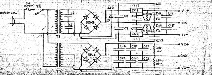
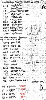
I see some "systemic" things that bother me, but I am no expert at discrete design. So, while I have it disassembled, I'd like to get some input on how to improve it. I have attached scans of the only available info for it: amp channel, power supplies, and parts list. Note some error corrections in red on the parts list.
Right now both channels work but have 250-350mV of DC offset after warmup. So far I have:
: replaced all the 'lytics and carbon comp resistors, some of which had gone well out of tolerance.
: verified all the power resistors ( > 1/2W ) are good.
: Matched the 1k2 R's to the input pair within 1 Ohm.
I'm also adding a dual 10k pot at the input.
My amp mostly matches the schematic but not exactly. On mine, Q1 and Q2 are 2N5651's. There is no trim pot between Q5 base and emitter. C5 is 100nF. At the inputs, the 2R2 is 2R7 on mine. C12-C15 in the ps are now diodes (correctly oriented). (There may be other differences I haven't noticed)
Things that bother me that I will be addressing:
: some ps distribution asymmetry in the layout.
: very little capacitance on the regulator adjust pins and outputs.
and then
: standing the channel grounds off power ground by 2R7 (why?)
: gain is much higher than needed
Without altering the basic design (space is limited on the pcb), what would you do to improve it?
Attachments

Last edited:
Trimpots on Q5 long term are unreliable. The pot wiper oxidizes, loses contact, and the idle bias on Q9,10 goes out of control and burns them.
Savvy designers find what pot value gives the correct idle current then replace the pot with a resistor. You haven't said what the current through Q9,10 emitter resistors is, which is a key measurement. Should be about 20 to 40 ma, or 2 to 4 mv. You'll have to put a pot b-e on Q5 to make adjustments, but after satisifed replace with fixed resistor again for long life.
BTW amps that live long lives in high wattage service have output transistor emitter resistor values of .33 or .51 ohms. At 1 - 2 watts in a living room, the .1 ohms shown may be okay, but next time I did a parts order I'd buy some .47 or .51 ohm wirewound 5 watt resistors. then replace the .1 ohm emitter resistors.
Most obnoxious reading is the 280 mv dc offset on output. >200 mv is generally unacceptable. I'd try a pot from whichever v1 rail is appropriate, to base of Q2, to try to adjust it out. Then later, a fixed resistor. Baking the q1 q2 section with a hair dryer while measuring the DC output may be useful, as the dc offset may be different at different temperatures. Finding a offset current that best reduces output DC offset at all temperatures is the goal. The voltage on higher value emitter resistors at 20-40 ma obviously would be higher by ohms law. Measure idle bias after the change and correct if necessary.
0.1 uf film cap is usual for C5.
If your amp has trouble with picking up radios, I'd put a 14 turn 14 ga wire wound around a 3/8" dowel (or AA battery, remove after winding) inductor between C5 & the output jack. Parallel a 6.8 to 10 ohm 3 watt resistor. The closer this inductor is to the output jack the shorter the antenna feeding RF into your Q2 base.
I see C2 on the input is there to short out RF from the input side. 390 pf is pretty substantial and may lessen high frequency response some. 150 pf to as low as 68 pf is more usual. Check for ultrasonic oscillation on the output if you change this, the large value C2 may be some sort of a patch for bad layout.
BTW 280 mv dc on output may really be ultrasonic oscillation as measured with a DVM. If you don't have a scope to check for that, I'd check output with an analog VOM with a 2v or 20 v AC scale. Put a .047 cap series the negative lead to block AC readings from DC volts. If a 280 mv AC reading occurs, check also with a 390 pf blocking capacitor. any AC that gets through a 390 pf capacitor is ultrasonic, and then compensation or layout redesign must begin. Which I won't get into.
As this is a direct connected amp, I'd buy some sort of DC protection board and apply it to the output. To disconnect the speaker on excessive Dc out. If your speakers cost more than $3.
Best of luck.
Last edited:
V2 should be lower and the one with the big caps, your red marks are erraneous
T2 is the bigger xformer
T2 is the bigger xformer
Trimpots on Q5 long term are unreliable. The pot wiper oxidizes, loses contact, and the idle bias on Q9,10 goes out of control and burns them.
Savvy designers find what pot value gives the correct idle current then replace the pot with a resistor.
Makes sense. Maybe that's why they removed the pot from this version.
You haven't said what the current through Q9,10 emitter resistors is, which is a key measurement. Should be about 20 to 40 ma, or 2 to 4 mv.
The bias adjustment spec is 25mA. Those resistors are inaccessible when the amp is assembled, so the bias adjustment instruction is to lift the -V2 lead, insert the mA meter, measure the idle current, adjust the 200R pot on the Q1 Q2 emitters to add 25mA, then do the same for the other channel.
You'll have to put a pot b-e on Q5 to make adjustments, but after satisifed replace with fixed resistor again for long life.
There is a 3k0 there now.
BTW amps that live long lives in high wattage service have output transistor emitter resistor values of .33 or .51 ohms. At 1 - 2 watts in a living room, the .1 ohms shown may be okay, but next time I did a parts order I'd buy some .47 or .51 ohm wirewound 5 watt resistors. then replace the .1 ohm emitter resistors.
Interesting info, thanks. What is the benefit of the lower value? Lower output impedance?
Most obnoxious reading is the 280 mv dc offset on output. >200 mv is generally unacceptable. I'd try a pot from whichever v1 rail is appropriate, to base of Q2, to try to adjust it out. Then later, a fixed resistor. Baking the q1 q2 section with a hair dryer while measuring the DC output may be useful, as the dc offset may be different at different temperatures. Finding a offset current that best reduces output DC offset at all temperatures is the goal. The voltage on higher value emitter resistors at 20-40 ma obviously would be higher by ohms law. Measure idle bias after the change and correct if necessary.
This is partially what confused me. I originally thought the Q5 b-e trimpot was to set bias current, and the 200R pot between Q1 Q2 was to trim offset. But that was blown when I saw this unit had no Q5 trim, and the 200R was used to set bias current.
0.1 uf film cap is usual for C5.
Yeah, I think that was just a parts list error.
I see C2 on the input is there to short out RF from the input side. 390 pf is pretty substantial and may lessen high frequency response some. 150 pf to as low as 68 pf is more usual. Check for ultrasonic oscillation on the output if you change this, the large value C2 may be some sort of a patch for bad layout.
Agreed. I saw the same and already lowered C2 to 220pF.
BTW 280 mv dc on output may really be ultrasonic oscillation as measured with a DVM.
There's no oscillation, it was quite a stable amp back when I used it. A little "dark" sounding but pretty solid.
As this is a direct connected amp, I'd buy some sort of DC protection board and apply it to the output. To disconnect the speaker on excessive Dc out. If your speakers cost more than $3.
Best of luck.
Many thanks. I'll consider that.
bansuri said:V2 should be lower and the one with the big caps, your red marks are erraneous
T2 is the bigger xformer
My markings in red are the measured values. V2 feeds the output stage; V1 is regulated at 32V for the drivers.
This switch in the feedback... if it wears or corrode... cheap and in time very sensitive for faults. DC offset can happen from there or when in bridge from the other channel (hopefully lifting it's output to the same dc level).Without altering the basic design (space is limited on the pcb), what would you do to improve it?
371/337 are simple, better options are readely available now, with more adjust pins control.
Make sure +/-V1 and +/-V2 returns ('grounds') are in prestine condition to avoid running away the references from signal grounds.
There is an essential initial current source missing in the Q3-Q6 current sources circuit part, at least a resistor to ground or +V1.
Lower value of output transistor emitter resistors gives higher wattage. As the ear is logarithmic, the difference between 39.8 and 39.9 watts is inaudible. Not worth taking the risk leaving them .1 ohms IMHO.Interesting info, thanks. What is the benefit of the lower value? Lower output impedance?
.
This switch in the feedback... if it wears or corrode... cheap and in time very sensitive for faults. DC offset can happen from there or when in bridge from the other channel (hopefully lifting it's output to the same dc level).
Good suggestion - I won't be using bridged mode, and will jumper the switch.
371/337 are simple, better options are readely available now, with more adjust pins control.
I've already replaced the LM317 with LT1085.
There is an essential initial current source missing in the Q3-Q6 current sources circuit part, at least a resistor to ground or +V1.
???
indianajo said:... output transistor emitter resistors... Not worth taking the risk leaving them .1 ohms IMHO.
I have some R39's here and will use them if they will fit...
Last edited:
More questions.
Is lowering the gain as simple as lowering the feedback resistor?
Why would the channel grounds be stood off ps ground by 2.7 Ohms?
Also I'd like some more input on the bias arrangement. It appears to me, in the schematic, the 5k pot on Q5 b-e was intended to set the bias, and the 200R on the input pair was intended to be an offset trim. Is that correct? But on later versions (this amp), a 3k6 resistor replaces the 5k pot, and the bias adjustment is done via the 200R pot. This appears to tie the output offset voltage to the bias adjusment. Since the amp will be driving a transformer-coupled transducer, I'd like to minimize the offset.
You could try shorting the 2.7 resistor & see if hum results. Many amps have ~3 to 10 ohms between the return of the output section, and the return of the input transistors, to avoid coupling large voltage changes into the input.Why would the channel grounds be stood off ps ground by 2.7 Ohms?
I would replace the 200 ohms pot between emitters Q1 & Q2 with two 100 ohm fixed resistors. Then you could change the values of collector & emitter resistor on Q1 to reduce the gain. Changing overall feedback may increase distortion, as transistors are inherently exponential current amps, and are only linearized by resistor ratios. Too little global feedback increases harmonic distortion. Too much global feedback lowers slew rate. and if the phase of feedback approaches 360 degrees, the amp oscillates instead of amplifying.Is lowering the gain as simple as lowering the feedback resistor?
As said before, I would feed current from a rail voltage into base of Q2 to move the DC offset to zero.
You may alternately feed a little current through a resistor from the output to some inverting high gain point, like the emitter resistor of Q2. To provide negative response to dc on output. this should be capacitor filtered to make it work only on voltage below 1 hz. There is no emitter resistor on q2, it goes straight into the constant current source, to you would have to add resistors to q1 & q2 to make this work as a Dc offset feedback.
Rather than doing these design changes with a soldering iron, you may want to simulate using spice. I don't have windows or apple op system, so I don't use simulators. But I get what I want by copying schematics, I don't really have a desire to dive off into complete design. Been done 10000 times by others.
Last edited:
More questions.
Is lowering the gain as simple as lowering the feedback resistor?
Why would the channel grounds be stood off ps ground by 2.7 Ohms?
Also I'd like some more input on the bias arrangement. It appears to me, in the schematic, the 5k pot on Q5 b-e was intended to set the bias, and the 200R on the input pair was intended to be an offset trim. Is that correct? But on later versions (this amp), a 3k6 resistor replaces the 5k pot, and the bias adjustment is done via the 200R pot. This appears to tie the output offset voltage to the bias adjusment. Since the amp will be driving a transformer-coupled transducer, I'd like to minimize the offset.
You may encounter stability issues if the gain is to low.
The 200 ohm is as you say for DC offset adjustment. The 5k bias preset and the offset preset should work independently but a a high DC offset will skew the bias current result if you have a load attached.
The circuit would need more analysis but the DC balance (the circuit design) doesn't look optimal.
OK, thanks for your input, guys. I'll skip altering the gain, it's not that important. I'll put it back together and see where the offset is at now that the out-of-tolerance parts have been replaced.
Oh, one more thing. Shouldn't there be a small (say 22pf) capacitor across the 22k feedback resistor to limit the gain at high freq's? The feedback path is pretty long, around 8 inches.
Lower value of output transistor emitter resistors gives higher wattage. As the ear is logarithmic, the difference between 39.8 and 39.9 watts is inaudible. Not worth taking the risk leaving them .1 ohms IMHO.
Lower values of emitter resistors will also (at the same specified bias setting) produce quite a bit more standby heat as the idle current will have to proportionally increase to achieve the same bias voltage across the emitter resistors. This may not a non-trivial matter and should be kept in mind.
Q3, D1, D2 and Q6 (& the 226Ω resistor) act as a current mirror, but the initial current to mirrir is missing. As drawn in this way, Q3 and Q6 do not conduct any current.
It will limit the upper band to 330kHz, which is ok.Oh, one more thing. Shouldn't there be a small (say 22pf) capacitor across the 22k feedback resistor to limit the gain at high freq's? The feedback path is pretty long, around 8 inches.
I powered up the amp. After 45 minutes the output offset settled in at 130-140mA on each channel. An improvement.
So I started setting up to adjust the bias. While pulling the -V2 lead fom the diode bridge, my hand slipped and I apparently momentarily shorted one of the AC terminals to the -V on the bridge. Spark, but no smoke. I checked the DC at the outputs. Over 4V on both of them. Damn. I just made my life more difficult.
So I started setting up to adjust the bias. While pulling the -V2 lead fom the diode bridge, my hand slipped and I apparently momentarily shorted one of the AC terminals to the -V on the bridge. Spark, but no smoke. I checked the DC at the outputs. Over 4V on both of them. Damn. I just made my life more difficult.
My first time troubleshooting a discrete power amp, could use a little guidance. All of the semiconductors diode-test as expected in-circuit. I'm inclined to disconnect the 38V supply feeding the output stage, power up the preamp section and trace through it. Good approach?
Well, hindsight is wonderful. I thought pulling the wires off to measure the idle bias with an ammeter sounded risky. On an amp where there is no way to check idle bias because the factory transistors are all matched, I installed a cinch solder terminal strip with wires down to the emitter resistor so I could measure idle bias via voltage. I'm not paying the price for factory sourced transistors. I can measure the voltage remotely with the output transistor board installed. Had to fiddle with the diode stack & series resistors between drivers to get idle bias right.
I'd do a Iceo test on the output transistors. They sometimes pass a diode test at 2 v of a meter, but are too damaged to hold off rail voltage. So I put in series a 12 v power supply, a 47k resistor, the c to e terminals of the suspect transistor, and the microamp scale of the DVM. Base is left unconnected. If the current is 12v/47k, then the transistor is zorked. If much less, it will hold off 12 v c to e. That is for npn, for pnp you put -12 v c to e.
Or since there are only 2 of them, you could just replace the output transistors. ~$8 + freight from newark, mouser, or digikey.
Last edited:
I powered up the amp. After 45 minutes the output offset settled in at 130-140mA on each channel. An improvement.
So I started setting up to adjust the bias. While pulling the -V2 lead fom the diode bridge, my hand slipped and I apparently momentarily shorted one of the AC terminals to the -V on the bridge. Spark, but no smoke. I checked the DC at the outputs. Over 4V on both of them. Damn. I just made my life more difficult.
First thing to do would be to make sure you are now using a DBT (dim bulb tester) to save any more disasters.
You then need to make sure ALL supply voltages are reasonably correct although they may be a little low if the bulb starts to light.
Having both channels with a 4 volt offset suggests a common cause such as a rail problem somewhere.
- Home
- Amplifiers
- Solid State
- Improving an old power amp