Hello Folks,
I have a B&K ST-202 that’s in great physical shape but thus far 1 channel has all MOSFETs dead and the other channel may have some leaking as well since it has +65 VDC at the output, I haven’t checked anything else because I’m trying to decide if it’s worth fixing due to the rarity and cost of the MOSFETs and the fact that I paid too much for it haha, so I’m reading many posts with contradicting information about these MOSFETs, some say they can be replaced, some say that don’t, some say they’re lateral, some say they’re not...
I even found a long thread but that was supposedly an ST-202+ even when it looks exactly like mine except for the toroidal being shielded. Anyway...
So has anybody actually replaced these 2SJ115 and 2SK405 with the 2SJ200/201 and 2SK1529/30?
If so, are they direct replacements or did you have to modify something else?
Perhaps completely replaced them with something totally different?
Any other ideas?
Thanks,
Alex
Last edited:
Hi Alex,
Yes, I just repaired one. And yes, the MOSFETs had to be replaced on one channel. Here is what I think the design flaw is on these amps: the ground connector on the main circuit board goes through a 4-pin connector. As time goes on, this connector oxidizes. And when it does, the feedback loop and DC balance goes nuts and blows the outputs... Rotten design.
SO, here is what I did:
- Bought new 2SJ115 and 2SK405 from a reputable NOS supplier (I just cannot remember who it was).
- Replaced the source resistors - I think they are .22 ohm - 5W or so - as many of these had fried when the amp blew up.
- Replaced any other burned resistors on the output PCB.
- Finally: soldered a permanent ground connector to the central ground point from each amplifier section on the main board. Best place to tab that is where the 4-pin connector lands on on the main board. This way, any iffy connection in the 4-pin connector willl no longer cause trouble.
Good luck!
D.
Hi Alex,
Disregard the last post; It was a EX-442 I fixed.
Looking at your pictures, it appears that the ST-202 you have here is an evolution of the ST-140: PlayAgainAudio: Reparing B&K ST-140 Mosfet Power Amp
That is good news. As we can make use of other MOSFETs in the output with a little creativity. While 2SK1580 and 2SJ162 has the source and drain pins reversed, they may be easier to get and will likely work in this amp.
The BIAS setting may very well be different. So if you try with other MOSFETs, make sure you turn the BIAS pot to the lowest setting before firing it up.
Now, if you want to be more methodically about it, we can try to get the boards up an d running without MOSFETs - but that involves soldering in 2 47K resistors from the collectors of the driver transistors to the base of the long tail pair of the input transistors - at the point where the 24K feedback resistor normally is connected. Don't worry, you don't need to remove that resistor since we now have eliminated the output MOSFETs.
The two 47K resistors from the collectors of 2n5416 and the 2n3446 acts as feedback for now. What we should see here is 1-2V across the BIAS pot. If so, all is fine. If not, we need to dig deeper...
Man - I need glasses... 2SK1058 and 2SJ162. These should work - if you swap the DRAIN and SOURCE pins. The GATES still go to where the gate stopper resistors are.
D.
D.
If the source and drain pins are swapped then that suggests one is a lateral mosfet and other is vertical mosfet.
GDS is vertical and GSD is lateral, usually !
GDS is vertical and GSD is lateral, usually !
Hi Alex,
Soldering in 2 47K resistors from the collectors of the driver transistors to the base of the long tail pair of the input transistors - at the point where the 24K feedback resistor normally is connected. Don't worry, you don't need to remove that resistor since we now have eliminated the output MOSFETs.
The two 47K resistors from the collectors of 2n5416 and the 2n3446 acts as feedback for now. What we should see here is 1-2V across the BIAS pot. If so, all is fine. If not, we need to dig deeper...
Hello vilfort,
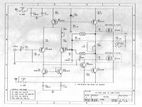
Thanks for jumping in to help, I'd like to do what you suggest but I have never done something like that before and the part numbers you are referring to do not match with the version of the amplifier I have, I'm attaching the schematics of this version, can you please let me know from where to where do I need to solder the resistors?
Thanks again!
Alex
Attachments
GDS is vertical and GSD is lateral, usually !
Thanks nigelwright7557, I'm still not sure these are Lateral, I have seen a bunch of contradicting posts, is there another way to test if they are?
Because the pinout is normal GDS, attached are the Old Datasheets...
Attachments
Helper resistors for trouble-shooting
Hi Alex,
The two 47K resistors are soldered on the board temporarily while ALL the output MOSFETs are out of the circuit.
The voltage across the BIAS pot P2 should be ~ 1.2V or so. And the voltage on either side of P2 relative to ground should be .4V to .8V or so +/-.
If you get crazy high voltages - like 20V or even 60V - around the P2 pot relative to ground, we have a sick board on our hands and it is time to dig deeper. The benefit of the 47K helper resistors is that they provide the needed feedback for us to trouble-shoot the input and VAS stage without frying expensive MOSFET outputs.
Let me know how it goes and what you find.
D.
Attachments
Hi Alex,
Many fake parts out there (sanded down cheap MOSFETs re-branded as real Toshiba parts). But these look right: 4 X GENUINE EARLY TOSHIBA 2SK405 2SJ115 POWER MOSFET | eBay
But prices are high... <sigh!>
Many fake parts out there (sanded down cheap MOSFETs re-branded as real Toshiba parts). But these look right: 4 X GENUINE EARLY TOSHIBA 2SK405 2SJ115 POWER MOSFET | eBay
But prices are high... <sigh!>
OK, so I have followed your advise and added the 2 47K resistors and this is what I got:
Channel 1 - Left side from Front
The voltage across the BIAS pot P2 is 1.93V
P2 Side 1 Relative to GND is - 1.03V
P2 Side2 Relative to GND is +0.9V
DR LED is ON
Channel 2 - Right side from Front
The voltage across the BIAS pot P2 is 1.928V
P2 Side 1 Relative to GND is +21.3V
P2 Side2 Relative to GND is + 23V
DR LED is ON
Looks like Channel 1 is Good but the strange thing is that this channel got all 3 pairs of MOSFETs fried... and Channel 2 seems to have something else going on but the MOSFETs pass the diode and component reader tests.
I guess I'll have to check the other transistors now...
Alex,
Did you use the same ground point for both measurements?
Nope, I used their respective ground speaker binding post for each measurement, they both come from a chassis central ground.
Hi Alex,
This is good news - and bad news (not really a big deal 🙂 ).
Don't fret over the state of the amp. Who knows what wildness it had to endure before you obtained it. Assume nothing...
First the good news:
Channel 1 is what we want. This channel seems OK. You may connect either side of P2 to a scope and see what a sine and square signal looks like - but that assumes you have a scope and a signal generator. Since I don't know if that is true, let's proceed with just using a voltmeter.
The goal now is to get the second channel to come up the same way as channel 1.
The two driver transistors 2n5416/2n3440 is expected to both conduct and create a balanced midpoint across P2. This is not happening on channel 2. So the next step is to de-solder these two transistors and test them with the meter. I hope your meter has
a diode test setting. With this, test BASE to EMITTER and BASE to COLLECTOR. You should see ~ 300-500 or so on the display - and no shorts. Then test COLLECTOR to EMITTER and no shorts.
If any of the two driver transistors are found to be faulty, then replace. But before we solder the drivers back in, test ALL resistors on the board.
Also: remove Q6 and test with the same diode test as above. While Q6 is out of the board, ground R6 (the leg that goes to the output) and test voltages around Q1,Q2,Q3,Q4 and Q5. Then compare these voltages to Channel 1's voltages.
At this point we should have a good sense of what is broken.
Please let me know your findings - we are close!
D.
Hey D.!
Well good news, I did all the testing you suggested and more, I basically ended up unsoldering every transistor in the board and they were all good, soldered them back and the problem was still there, then I removed all electrolytic caps and tested them for Value, ESR and Leakage at their rated voltage, they are all good except for the Input coupling ones which are supposed to be 47uF but they are ~67uF but not bad ESR nor leakage at their rated voltage, since I don't have any NP 47uF caps in hand I soldered them back. I guess I should change them...
I tested all resistors and well, again, all good, so I ended up reflowing every solder joint in the board and tested continuity across all joints and connected all back, voila!
Now these are the values I have, I guess cold solders or something...
Channel 1 - Left side from Front
The voltage across the BIAS pot P2 is 1.93V
P2 Side 1 Relative to GND is - 1.03V
P2 Side2 Relative to GND is +0.9V
DR LED ON
Channel 2 - Right side from Front
The voltage across the BIAS pot P2 is 1.915V
P2 Side 1 Relative to GND is - 1.027V
P2 Side2 Relative to GND is + 0.893V
DR LED ON
Now the question is, what MOSFETs should I use?
I did take a chance and bought some pairs of supposedly original pulls of Toshiba 2SK1529 / 2SJ200 that should arrive in a couple of weeks or so, do you think those would do the trick?
Thanks,
Alex
Hi Alex,
That is good news indeed! You now have two boards that are both working.
From looking at the the datasheets, it appears that 2SK1529 and 2SJ200 would work. They look very similar to the originals - except they are 180V versions rather than 160V. You are at 120V in this amp - so give it a whirl.
But, as long as you have 2 of each of the 2SJ115 and 2SK405 you CAN get the amp up and running for testing with just one pair in each channel. But don't crank the amp or run any low impedance speakers without all 6 MOSFETs in each channel. If you want to test this with just 2 MOSFETs in each channel, extra precaution should be taken by running 1A FAST fuses on the rails temporarily.
You are close to having it all up and running again! - Good luck.
D.
Definitely looks like an evolution of the ST-140. The ST-140 used a pair of TO-3 laterals, I want to say it was 2SK135 and 2SJ50.
I call these amps blimps because they're physically rather large, but almost completely empty inside. It's one of those devices that really could have (and should have) been a 2U enclosure, but someone decided to make it a 3U.
I call these amps blimps because they're physically rather large, but almost completely empty inside. It's one of those devices that really could have (and should have) been a 2U enclosure, but someone decided to make it a 3U.
Thanks to you D. your help has been one of the best kind I have ever received in this fantastic community.
I will test with only one pair as you suggest and then wait for the MOSFETs I ordered and see how it goes.
If you look at the pictures the boards come prepared for 5 pairs each rather than 3, they even have the resistors already installed and the heathsinks are also ready, I’m wondering what would happen if I install 5 pairs?
Perhaps the power supply will fall short?
The ST-202+ version has a beefier shielded Toroidal that puts +/- 75V rather than +/- 63V but it also has only 3 pairs installed, weird...
Definitely looks like an evolution of the ST-140. The ST-140 used a pair of TO-3 laterals, I want to say it was 2SK135 and 2SJ50.
I call these amps blimps because they're physically rather large, but almost completely empty inside. It's one of those devices that really could have (and should have) been a 2U enclosure, but someone decided to make it a 3U.
Hahahah, yeah they are “Meetings that should have been an email “...
I also have an ST-140 that needs some TLC, I will look at it once I fix this one, that one works but at idling and low volume all is fine but as soon as you crank it up it puts 1-2 VDC Offset...
I’m wondering if it just needs new Electrolytic Capacitors, we’ll see...
Hi Alex,
Thank you for the kind words. Much appreciated.
These 'bread boxes' are indeed full of air (that blimp comment was funny!). But that also means that there is plenty of room for creative modifications. I took a ST-140 and made it into a great sounding hybrid with 4 6SN7's driving two pairs of 2SK1058/2sj162. Sounded good and the "blimp" had plenty of room for the 400V power supply and the tubes...
Back your question: sure, you could go with 5 MOSFETs X 2. But you don't need it. As a rule of thumb: 1A per MOSFET. And at 63V, more than 3 is not needed - unless you want to drive 2 ohm speakers... And also remember that MOSFETs do have capacitance, - so the more you parallel, the more aggregated capacitance you need to drive. This affects slew-rate. Stick with 3. But there is really not any harm in trying 5 if you have enough MOSFETs at hand (still, that is easily $14 X 8 = $112 extra cost).
The power supply can likely handle the draw - but remember that the heatsinks are rather small and running 5 MOSFETs will suck ~550mA idle current. You might get away with it - but things will get toasty.
About the ST-140: use the same 47K X 2 helper resistor approach to trouble-shoot the amps driver boards. Remember to remove the 2SK135/2SJ50's when doing so.
Good luck. And please let us know how it goes.
D.
Ok so after 3 weeks I finally got some 2SK1529 and 2SJ200 pairs that seem to be authentic, I'm wondering what type of matching method could I be using here since I don't have a Curve Tracer.
Would this simple method work?
Any other Ideas?
Thanks Again!!
Would this simple method work?
Any other Ideas?
Thanks Again!!
- Home
- Amplifiers
- Solid State
- B&K ST-202 Repair