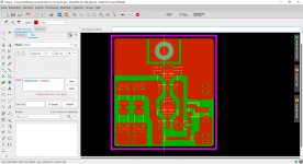
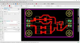
Good components placement for good results.
Ake, try again!
Jan, you‘re right, net classes (width, clearance) are possible settings in EAGLE.
JP
Ake, try again!
Jan, you‘re right, net classes (width, clearance) are possible settings in EAGLE.
JP

I am quite sure that with net classes proper set even the autorouter would not try to route a 500V track between two smd pads. Before any routing
-Do spend much time on ultimate component placement
-Do setup your design rules.
For about 30yrs I do PCB-CAD now. Never touched any autorouter.
-Do spend much time on ultimate component placement
-Do setup your design rules.
For about 30yrs I do PCB-CAD now. Never touched any autorouter.
Last edited:
The problem is that the autorouter has no idea of voltage, of what '500V' even is ;-)
The thing to do is to assign the 500V line to a class 'highvoltage' and then set the design rule for class 'highvoltage' to say 20mills clearance.
Jan
The thing to do is to assign the 500V line to a class 'highvoltage' and then set the design rule for class 'highvoltage' to say 20mills clearance.
Jan
Attachments
Last edited:
Certainly. I assume proper net classes for 500V lines. These considerations are the same for manual- or auto-routing.
Is there anything wrong?I tried not to place the components to close.Good components placement for good results.
Ake, try again!
Jan, you‘re right, net classes (width, clearance) are possible settings in EAGLE.
JP
Is see that I can mover one Led and maybe the 4 resistors.
Why not on heatsink?
Find EAGLE files attached: net class for 500V defined:
Leiterbahnabstande – Mikrocontroller.net
JP
Find EAGLE files attached: net class for 500V defined:
Leiterbahnabstande – Mikrocontroller.net
JP
Attachments
I think you should not worry too much about board size at this point (yes I know I commented on it ...).
Try to get a feel for better layout. As noted, repetition makes you a master.
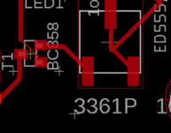
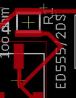
Example: in pic 1, rotating the transistor and moving it and the cap (?) that is at it's right lets you run that thin track between the cap pins.
In pic 2, it seems you have a weird track to connect two points that are next to each other.
Also, rotating both LEDs 90deg CCW will make the tracking shorter.
Jan
Try to get a feel for better layout. As noted, repetition makes you a master.
Example: in pic 1, rotating the transistor and moving it and the cap (?) that is at it's right lets you run that thin track between the cap pins.
In pic 2, it seems you have a weird track to connect two points that are next to each other.
Also, rotating both LEDs 90deg CCW will make the tracking shorter.
Jan
Attachments
Last edited:
In pic 2, it seems you have a weird track to connect two points that are next to each other.
Also, rotating both LEDs 90deg CCW will make the tracking shorter.
Opps din´t see that.
Also, rotating both LEDs 90deg CCW will make the tracking shorter.
Opps din´t see that.
Why not on heatsink?
Find EAGLE files attached: net class for 500V defined:
Leiterbahnabstande – Mikrocontroller.net
JP
It is a little unfair .what takes you 2 minutes to do takes me 1 day....😎
Some of the footprints have silk screen running over the copper pads.Moved the transistor..
As silk screen is done last you will end up with silk screen on your pads which might make it hard to solder.
It is a little unfair .what takes you 2 minutes to do takes me 1 day....😎
Yes it is. Also that other stuff you didn't see, that is quite normal. I can't tell you how often I finished a PCB, being quite proud of myself, then looked at it a few hours later and ask myself how I could be so stupid ;-)
It gets better with every layout, especially when you start to learn the program and you are no longer distracted by cursing because you can't find the right command.
You're doing fine.
Jan
Some of the footprints have silk screen running over the copper pads.
As silk screen is done last you will end up with silk screen on your pads which might make it hard to solder.
Do you mean the components txt that is on the board?
I checked at JLC pcb´s site that I wont be on the finished board .
Following data using EAGLE 9.5.2 CAM-Prozessor are to supply for manufacturing:
- top layer (1)
- bottom layer (16)
- top stop layer (29): you´ve to drawn the outline again on this layer, width =0,6mm
- bottom stop layer (30): you´ve to drawn the outline again on this layer, width =0,6mm
- top silkscreen depends on components definition (layer 21, 25, perhaps 27?)
- outline (20)
- top cream (31) if you want reflow mask
- plated and non plated drill datas
No silkscreen information over electrical pads.
JP

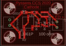
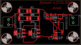
MUCH better! But still some track width irregularities for N$1 at J1 and R2.
I would also recommend removing the part values, only leave the designations, and make sure no text is over the holes or too close to the holes.
Otherwise you will not be able to read it on the finished PCB.
Edit: also would be good if you could align the mounting holes with each other, helps with the holes later.
Jan
Last edited:
- Home
- Design & Build
- Equipment & Tools
- Eagle question