The seemingly never-ending saga of my JLH Monoblocs continues...😱
Both Power supplies are 100% now....and +/- 50V and 55V rails working as they should be 🙂
So...I'm now at the "Power Amplifier Setup" step in the user manual.
DMM set for mA...I've inserted meter into +55v rail....but there is NO CURRENT when switched on.
Circuit diagram is here....https://i.imgur.com/wCcCg5j.jpg
(Pencil annotations not mine....an on-line scan was the source)
Another...better circuit diagram can be found here...scroll almost 1/2 way down, circuit labelled "JLH 80W Mosfet...."
A Paul Kemble web page - JLH mosfet amplifiers.
I am given to understand that the driver may be at fault.....is that Q10 VN1210M? Can these devices be tested 'in-circuit'....or must they be removed please??
All info. gratefully received.....I will get there in the end😀
Basic initial measurements are to confirm the DC offset is actually zero irrespective of bias current. That test also goes a long way to confirming the driver is OK.
What is the voltage across the 56 ohm in the current source?
The voltage across Q8 should alter with the bias preset. You only need around 0.6 to 1 volt to turn the output stage on.
What is the voltage across the 56 ohm in the current source?
The voltage across Q8 should alter with the bias preset. You only need around 0.6 to 1 volt to turn the output stage on.
Basic initial measurements are to confirm the DC offset is actually zero irrespective of bias current. That test also goes a long way to confirming the driver is OK.
What is the voltage across the 56 ohm in the current source?
The voltage across Q8 should alter with the bias preset. You only need around 0.6 to 1 volt to turn the output stage on.
I'm getting 1.08v across R12 (56R)
That sounds very high... it should be no higher than around 0.65 volts, the B-E volt drop of any small silicon transistor (Q11 here). Q11 B-E should clamp the voltage at that level.
Although that needs investigating, it would actually tend to give to much bias current, not to little or none at all. You should have approx 0.65 volts giving a current of 11 milliamps in the VAS stage.
(oscillation could give misleading static DC readings)
Although that needs investigating, it would actually tend to give to much bias current, not to little or none at all. You should have approx 0.65 volts giving a current of 11 milliamps in the VAS stage.
(oscillation could give misleading static DC readings)
Is that implying that Q11 could be iffy???That sounds very high... it should be no higher than around 0.65 volts, the B-E volt drop of any small silicon transistor (Q11 here). Q11 B-E should clamp the voltage at that level.
Although that needs investigating, it would actually tend to give to much bias current, not to little or none at all. You should have approx 0.65 volts giving a current of 11 milliamps in the VAS stage.
(oscillation could give misleading static DC readings)
Remove and test....or am I jumping in here??🙂
Maybe jumping in... but the reading of over 1 volt DC across a B-E junction is definitely wrong.
If the transistor is OK and fitted correctly then only the presence of unwanted AC (such as instability/oscillation) could give such a reading. A scope would prove/disprove that in seconds.
Those two transistors form a classic ring of two current source. When the voltage across the 56 ohm reaches around 600 to 700 millivolts it turns on Q11 which then shunts base current away from Q9 thus limiting the current (and keeping it constant).
The 0.6 to 0.7 volts is a cast in stone figure. It's non negotiable in transistor terms 🙂
Should also add that....BOTH monoblocs aren't working....but different faults it appears.
Went to the 2nd amp...#2...and reads 0.67V across R12 (56R)....so a different prob with this one!!
Going to 'jump in' with first amp...#1...and test Q11 (BC214)....🙂
Went to the 2nd amp...#2...and reads 0.67V across R12 (56R)....so a different prob with this one!!
Going to 'jump in' with first amp...#1...and test Q11 (BC214)....🙂
OK...sticking to #1...tested (Q9) BC214....looks OK
Also tested (Q11) BF870 (with Base pin3) seems to test OK too.
Also tested (Q11) BF870 (with Base pin3) seems to test OK too.
The circuitry around Q9 and Q11 is self contained. Nothing connected to it (to the collector) can pull more current that the magic 0.6 to 0.7 volts allows.
The only exception is as I mentioned earlier and if the stage was oscillating. Then a DVM reading is meaningless. I wouldn't rule that possibility out tbh.
The only exception is as I mentioned earlier and if the stage was oscillating. Then a DVM reading is meaningless. I wouldn't rule that possibility out tbh.
VN1210M is a MOSFET. The circuit on the link to Paul Kemble is the Wireless Word JLH one from 1981 which I built around that time . There was a subsequent design using a VN1210M that first appeared in 1984 in ETI magazine.
Last edited:
It's clearly labelled as being from ETI/Hart '89-'96 and has the VN1210M, as my K1100M's have!!VN1210M is a MOSFET. The circuit on the link to Paul Kemble is the Wireless Word JLH one from 1981 which I built around that time . There was a subsequent design using a VN1210M that first appeared in 1984 in ETI magazine.
Are you looking at another circuit on the Kemble page perhaps??
The circuitry around Q9 and Q11 is self contained. Nothing connected to it (to the collector) can pull more current that the magic 0.6 to 0.7 volts allows.
The only exception is as I mentioned earlier and if the stage was oscillating. Then a DVM reading is meaningless. I wouldn't rule that possibility out tbh.
Not at all sure how to move on from this. Still in a position where I can't set the (is it 'quiescent'?) current in setup of the power amp(s)
OK, well lets work on the basis that while we know the measurement you have made is incorrect, it is incorrect in a way that should allow even more quiescent current (correct term 🙂) to flow.
You need to measure the other two items I mentioned earlier which were DC offset and voltage across Q8 as the preset is turned.
In particular, what is the highest voltage achievable across Q8 (from C to E)?
You need to measure the other two items I mentioned earlier which were DC offset and voltage across Q8 as the preset is turned.
In particular, what is the highest voltage achievable across Q8 (from C to E)?
Great....!!
As trim pot turned....voltage across Q8 spans 3.82v to 8.56v.
DC offset (at speaker terminals)....isn't stable....continuously falls
As trim pot turned....voltage across Q8 spans 3.82v to 8.56v.
DC offset (at speaker terminals)....isn't stable....continuously falls
This tells us something important... 3.8v to 8.5v should send the lateral FET's into oblivion. The voltage over Q8 should really go from close to zero to just a few hundred millivolts.
These devices begin to conduct at only around 0.2 volts gate to source voltage, much lower than even an ordinary silicon transistor.
So 8 volts across Q8 should be turning the FET's on so hard they short the supply (and fry at the same time) and I assume that is not happening...
You seem to have a lot going on with this I'm afraid.
You still haven't said what the offset is... is it close to zero or are we talking an offset of many volts?
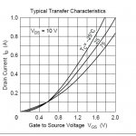
This shows the transfer characteristic of an N channel lateral FET. At 2 volts it is already conducting hard.
I really do wonder if your circuit isn't oscillating because your voltage readings (if they are true DC readings) don't really tally with what is happening. The FET's should be red hot with that voltage turning them on.
These devices begin to conduct at only around 0.2 volts gate to source voltage, much lower than even an ordinary silicon transistor.
So 8 volts across Q8 should be turning the FET's on so hard they short the supply (and fry at the same time) and I assume that is not happening...
You seem to have a lot going on with this I'm afraid.
You still haven't said what the offset is... is it close to zero or are we talking an offset of many volts?
This shows the transfer characteristic of an N channel lateral FET. At 2 volts it is already conducting hard.
I really do wonder if your circuit isn't oscillating because your voltage readings (if they are true DC readings) don't really tally with what is happening. The FET's should be red hot with that voltage turning them on.
Attachments
It's clearly labelled as being from ETI/Hart '89-'96 and has the VN1210M, as my K1100M's have!!
Are you looking at another circuit on the Kemble page perhaps??
Scrolling down from the 1980 circuit I see the 1984 one.
Apart from equivalent component number changes the 1989 one has some detail change in that a 10n lead capacitor has been added to the 39R source resistor of the VN1210M - this apparently to improve the gain bandwidth product and an output coil included for stability reasons.
The closed loop gain of this system is very high and in a later article in 1993 this was reduced.
I have the ETI issue for the 1989 version and that for the 1993 one which was in Wireless World? I am on holiday at present and don't have access to these. Wireless World changed their name to Electronics and Wireless World at some time.
The regulated power supplies for the 1989 circuit uses MOSFET power devices. Both the 1984 and 1993 circuits use Darlington transistors. Of these the 1993 is simplest and avoids complications you may get with MOSFET devices.
I am aware that MOSFET's can fail. I did some repairs as a favour for a friend who was the proprietor of a business using these devices in its' product range.
The business had left for the UK and and my friend remained here during the sale and removal of his home.
You can access virtually all issues of WW and E&WW from the original "Marconigraph" of 1911 up to 2005 and also many other worthy, English language electronics magazines online. It's a big site with a vast library of scans. This link should land you close enough for a focused search: WIRELESS WORLD: UK technical magazine 1913-2005
The article is in Electronics World + Wireless World issue of June 1993. For what it is worth this has a 10 V zener diode in parallel with C3 value 100pf as shown on page 32 in the May 1989 article. Also there is one complementary pair of output MOSFET devices.
Doubling up on these can lead to oscillation so if replacements are called for then maybe there are some devices with a power rating that is double that for SK134/5 and SJ49/50 that would avoid parallel leads to paired devices.
Doubling up on these can lead to oscillation so if replacements are called for then maybe there are some devices with a power rating that is double that for SK134/5 and SJ49/50 that would avoid parallel leads to paired devices.
It'....face the music time....for Me!!
Thanks to a 'local' member of the PFM forum, who offered 'scope' services yesterday....can now update on 'no current' situation with these monoblocs😱😱
It transpires that....my UNI-T 70D DMM....had actually blown an internal fuse to the input for mA......hence 'No Current'. (It had never occurred to me to attempt measurement via the A input.....aaaaggghhh
Additionally...and to further compound the error....I had inadvertently (after many stripdowns/re-assemblies) managed to finally CROSS the +/- rails of the 50v supply😱...and this had gone under the radar.
Somehow...a catastrophe was avoided....but this now explains the ludicrous voltage readings observed by Mooly..... 🙂🙂
In fact...Mooly said "You seem to have a lot going on with this I'm afraid."
....which was 10/10....!
So sorry about that....really!
With readings sorted.....and polarity of 50v rails corrected....setting up quiescent current was textbook (even for Me)😀
Thanks again for all inputs.

- Home
- Amplifiers
- Solid State
- No current flow in JLH 80W Mosfet power amp.