Do you mean it settles to -27 V when you wait for 100 ms or more? Is -27 V also the voltage at t = 0? If so, it is very different from ctrlx's plot.
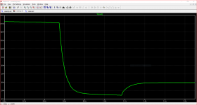
The image attached suggests the voltage gets down close to zero volts eventually. Running the simulation on 1kHz sine wave showed the dc persisted throughout. This also shows up on a dc operating point list. There is 150 odd m.A. of current passing through R10.
Attachments
Sounds like two bias points, a desired and an undesired one. Mjona, is Q3 in saturation in the undesired bias point? What input signal did you apply for the simulation of post 21?
Last edited:
Sounds like two bias points, a desired and an undesired one. Mjona, is Q3 in saturation in the undesired bias point? What input signal did you apply for the simulation of post 21?
PULSE(-0.1 0.1 0 5n 5n 50u 100u 10000) which gives a peak of over 20V with the IRFP's the peak is 5.52V on the same input.
I note the IFFPs have a zener diode included on the die whereas the 2SK and SJ types usually need an external one. None are shown on the .asc file.
If the latter are installed in the hardware then ctrlx might have said so - a point on which he has remained silent. We have not seen any 'scope images of his square wave results either.
So you start with -0.1 V, then you have a 10 kHz square wave during one second, then -0.1 V again. Apparently that suffices to get it out of the wrong bias point, if that's what it is. Does Q3 or Q4 saturate?
Last edited:
If there is spike because the loop gain is slower than the loop requires. The role of the stopper is to dissociate the capacitance as load for the precedent stage which may unstabilize it . Here the drivers are high impedance VAS, I don't see the idea of using stoppers.You know why gate stopper are there Kokoriantz ?
Could you explain your logic ---please ?
Here is a professional electrical engineering website advice on this
notice it reduces the speed and high frequency oscillations especially if long leads are used between the driver and actual gate.-
- Slow down the switching to reduce EMI.
- Reduce the current spike drawn from the supply during MOSFET turn-on. If local decoupling is not good enough, this current could make VCC sag, triggering the chip's UVLO. Fortunately the chip's pinout makes it easy to achieve a low inductance decoupling.
- In case the layout is suboptimal with a long gate trace. This adds inductance in the gate which can cause the MOSFET to osillate. A resistor will dampen the oscillations, at the cost of slower switching. This is a bit of
- a band-aid, a tight layout is preferable.
- They also reduce Ringing .
Last edited:
So you start with -0.1 V, then you have a 10 kHz square wave during one second, then -0.1 V again. Apparently that suffices to get it out of the wrong bias point, if that's what it is. Does Q3 or Q4 saturate?
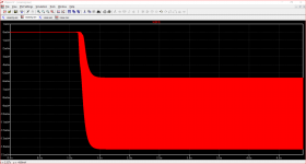
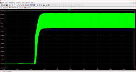
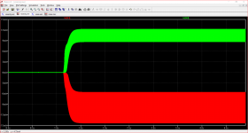
I ran the simulation for an increased number of cycles starting at 100ms and ending at 5 seconds. The plots for Q3 and Q4 are attached, also Q3 and Q4 together.
I have included my .asc file since the plot develops between t=0s and about 1.1s and this part shrinks as time increases. Those Q3 and Q4 Ic operating bands end up getting pretty thick.
Attachments
If there is spike because the loop gain is slower than the loop requires. The role of the stopper is to dissociate the capacitance as load for the precedent stage which may unstabilize it . Here the drivers are high impedance VAS, I don't see the idea of using stoppers.
We are talking about an overshoot spike on a 10kHz square wave that can be caused by loss of control .
This can be controlled ( in part ) by controlling the operating condition of a Mosfet just like I fitted grid stoppers long before mosfets/Jfets existed in valve (tube ) communications receivers to control RF oscillation in a high gain tube .
This is old school technology .
Not once did I change the values of the zobel network to try to obtain my objective as it was designed to do a specific function , I modified other parts of the design even changing the layout-----it worked , its down to circuit design ---why compromise when a more stable outcome can be achieved permanently by circuit redesign ??
This amplifier needs a grounding capacitor the input bases. The loop gain phase in CFA requires the bases to be very low impedance . In the circuit , it is slowed down by 1.5k resistor, but the source impedance in real world is not 0 ohm. If a long cable is used, the inductance is sufficient to run the amp into resonance. By adding a grounding capacitor the current feedback loops through grounded bases in HF. Unwillingly , the 1.5k resistor necessary to disengage the source from capacitive loading and the capacitor form an RF filter.
mjona, the file in post 1 works and M1/2 are b.cordell models.
if you change the devices you may need to adjust R11/12 or use 2mA currents.
the .asc file is missing several refinements but these are employed in the real cct.
i am currently evaluating the cct using the devices i already have but see the threads below for more details:-
VSSA Lateral MosFet Amplifier
PeeCeeBee
i am evaluting the cct without the input filter to see how well it copes dealing with a 10KHz square, once this has been "optimised" a 220pF will be used.
mjona, the file in post 1 works and M1/2 are b.cordell models.
if you change the devices you may need to adjust R11/12 or use 2mA currents.
the .asc file is missing several refinements but these are employed in the real cct.
i am currently evaluating the cct using the devices i already have but see the threads below for more details:-
VSSA Lateral MosFet Amplifier
PeeCeeBee
i am evaluting the cct without the input filter to see how well it copes dealing with a 10KHz square, once this has been "optimised" a 220pF will be used.
Your problem is mainly due to substituting BD139 and BD140 with MJE340 and MJE350 and the addition of C5 and C6. The former types were used in the vssa source link you provided.
Q3 and Q4 are common emitter amplifiers which invert the input signal and amplify whatever capacitance exists between the collector and base whether external or within the diffusion. The amplified capacitance will appear as a load on the bases of Q3 and Q4 needing to be driven by Q1 and Q2.
You can look at CJC in the .models used for BD139 and BD140 and compare these to those for MJE340 and MJE350 you will get some idea of quantifying the loads on Q3 and Q4 bases.
If you have a slew rate limiting problem due to the magnitude of the capacitance loading Q3 and Q4 base the presence of C5 and C6 makes matters worse.
In a roundabout way you have understood the need to increase the operating current in Q1 and Q2.
When I substituted the lower diffusion capacitance types BD139 and BD140 in your simulation file the problem disappeared without reducing R11 and R12.
If you have not adopted these in your list of several refinements there are good reasons to do so.
I used Bob Cordell's .models in my simulations. The link on my files references back to his website where full detail of his .models can be accessed.
Last edited:
I've simulated the operating point of the circuit of the .asc file of post #26 with the Bob Cordell models, and even though LTspice doesn't give any warnings about convergence issues, it looks like there is some numerical problem or a modelling issue related to Q4. The results are totally unphysical and become normal again when reltol is reduced to 0.0001.
The simulated DC output voltage with the default reltol of 0.001 is -27.1038 V. Q1 is off (collector current -35.1612 pA) and Q4's collector, base and emitter are at -36.3855 V, -36.2871 V and -36.8024 V with respect to ground, respectively. Although the base is slightly above the collector, it is probably not far enough to cause phase inversion due to hard saturation of Q4.
Q4 has a current of 153.246 mA flowing into its collector and a current of 7.89976 mA flowing out of its base, even though it is an NPN. NPN transistors can have large negative base currents due to avalanche effects when the collector-base voltage is higher than BVCEO, but when there is hardly any voltage across the device, it makes no sense at all.
Using reltol=0.0001 changes the DC output voltage to -0.115966 V.
I've simulated the operating point of the circuit of the .asc file of post #26 with the Bob Cordell models, and even though LTspice doesn't give any warnings about convergence issues, it looks like there is some numerical problem or a modelling issue related to Q4. The results are totally unphysical and become normal again when reltol is reduced to 0.0001.
The simulated DC output voltage with the default reltol of 0.001 is -27.1038 V. Q1 is off (collector current -35.1612 pA) and Q4's collector, base and emitter are at -36.3855 V, -36.2871 V and -36.8024 V with respect to ground, respectively. Although the base is slightly above the collector, it is probably not far enough to cause phase inversion due to hard saturation of Q4.
Q4 has a current of 153.246 mA flowing into its collector and a current of 7.89976 mA flowing out of its base, even though it is an NPN. NPN transistors can have large negative base currents due to avalanche effects when the collector-base voltage is higher than BVCEO, but when there is hardly any voltage across the device, it makes no sense at all.
Using reltol=0.0001 changes the DC output voltage to -0.115966 V.
It looks like you are onto something here. I downloaded ON Semiconductors Pspice model for MJE340 which behaves properly in the simulation.
Simulation Models: MJE340
There is no low pass filter on the input to limit the input frequency to a level the circuit can handle. Bonsai alluded to this out in post 3.
Slew rate is measured in V/uS so you are asking for 5.4V peak in next to zero time - a microscopic fraction of 1uS. If you invert time you get the frequency you are calling for - it looks to be astronomical.
Slew rate is measured in V/uS so you are asking for 5.4V peak in next to zero time - a microscopic fraction of 1uS. If you invert time you get the frequency you are calling for - it looks to be astronomical.
hi mjona,
just to clarify, with no input filter and no zobel a 10KHz square is very clean.
the addition of a zobel of 100n+10R (but no input filter) alters the square as shown in post 1.
using a input filter of 220p (but no zobel) the corners of the square are now rounded off....however if now the zobel is added some peaking returns.
futher tests have shown that a zobel of 1n+10R is the smallest cap not to effect the waveform (caps above this value have an effect)
It depends on the power amp circuit as to how it reacts to real life use with loudspeakers .
Impedance rises with frequency I would keep that (1n) value as it will flatten out the impedance.
Impedance rises with frequency I would keep that (1n) value as it will flatten out the impedance.
hi mjona,
just to clarify, with no input filter and no zobel a 10KHz square is very clean.
the addition of a zobel of 100n+10R (but no input filter) alters the square as shown in post 1.
using a input filter of 220p (but no zobel) the corners of the square are now rounded off....however if now the zobel is added some peaking returns.
futher tests have shown that a zobel of 1n+10R is the smallest cap not to effect the waveform (caps above this value have an effect)
I have not had much experience with MOSFET amplifiers having build only one of these 30 years ago.
Anyway, in his book " Valve and Transistor Audio Amplifiers" Linsley-Hood commented about source follower types - to the effect that for the avoidance of possible spurious HF oscillation not only must gate stopper resistors be used, but the MOSFET source electrodes must be protected from capacitative loads.
Wire-wound resistors 0R22 were used in the illustration with a comment that the small inductance in these would serve that purpose adequately.
How about this: just build the darn thing...🙂
I have - sounds OK - with 2SK1058/2SJ162. If you like, you can add spreader pot between the the two driver transistors for bias and then parallel with another pot with 10K to ground for DC balance. Forget simulations. Build something! Then listen.
I have - sounds OK - with 2SK1058/2SJ162. If you like, you can add spreader pot between the the two driver transistors for bias and then parallel with another pot with 10K to ground for DC balance. Forget simulations. Build something! Then listen.
According to the opening post and post 20, it has already been built: "in sims and real life", "i varied the zobel cap C1 in LTspice. a value of 10nF gave a quite good 10KHz square. in the real circuit, a value of 22nF is giving a very good 1 and 10KHz squares.." I don't know why the maximum Zobel capacitance for a good square wave response dropped from 10 nF...22 nF to 1 nF in later posts.
Last edited:
ctrlx, this whole thread is about a small (and in my opinion rather harmless) aberration in the step response, but did you also look at the real part of the output impedance as a function of the Zobel capacitance?
It's difficult to measure without an impedance analyser, but easy to simulate: remove the load and connect a unit AC current source to the output, making sure it is directed from ground into the output, run an AC simulation and look at the real part of the output voltage. When the real part of the output impedance is greater than or equal to zero at all frequencies and the amplifier is stable for some passive load, then the amplifier will remain small-signal stable with any passive load. Unfortunately there is no guarantee that the same holds under large-signal conditions.
It's difficult to measure without an impedance analyser, but easy to simulate: remove the load and connect a unit AC current source to the output, making sure it is directed from ground into the output, run an AC simulation and look at the real part of the output voltage. When the real part of the output impedance is greater than or equal to zero at all frequencies and the amplifier is stable for some passive load, then the amplifier will remain small-signal stable with any passive load. Unfortunately there is no guarantee that the same holds under large-signal conditions.
Last edited:
- Home
- Amplifiers
- Solid State
- vssa squarewave response