Hi all.
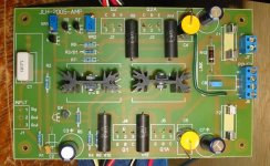
I build jlh 2005 using Paulb circuit and pcb. Now i face issue sound is too low. Use +-30v supply range. And use 2sc5200 for power output. 2 pcs 2sc5200 already died cause over bias(sad)
I double check hfe value for bc560, bd139 and bd 140 all in good range.
I don't have oscilloscopes and signal generator to measure input output gain.
I would use +/-22 volts max (at 2 amps) and adequate heatsink. Otherwise you will keep killing those poor output transistors.
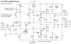
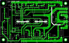
post sch and pictures of your build
Hi zen,
Original circuit prefer power output is Mj15003.But i use 2sc5200.
Can this replacement cause losses of amplifier gain?
Attachments
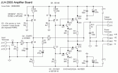
no, 2SC5200 is OK
your problem(s) lies elsewhere
you can measure gain precise enough, using PC program (plenty of them for free download) for sine signal , setting frequency to anything around 500Hz and using your DVM set to AC
DVM is good enough for that frequency
feed signal to your amp, set volume to read volt or so at output, then measure what's on input
divide and that's it
VR1, VR2 need to add fixed resistors between these and transistors bases!
Use 100R in series with, VR1 and 10R in series with VR2.
Use 100R in series with, VR1 and 10R in series with VR2.
Last edited:
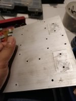
show us size of your heatsink, don't be shy!
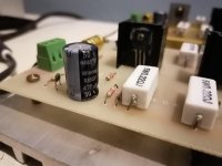
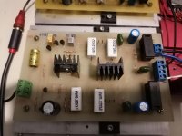
My heatsink 16x13cm temporary for trial version.
Thimios, i agree with you to add series resistor with this 2 vr for avoid over bias i think
Attachments
I use proteus software and it work to measure gain. In software gain is around 13..no, 2SC5200 is OK
your problem(s) lies elsewhere
you can measure gain precise enough, using PC program (plenty of them for free download) for sine signal , setting frequency to anything around 500Hz and using your DVM set to AC
DVM is good enough for that frequency
feed signal to your amp, set volume to read volt or so at output, then measure what's on input
divide and that's it
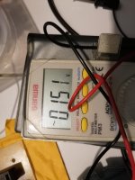
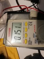
In actual i set 500hz at 0.15vac for input. And output also same.. Can refer picture. 1st picture for input and 2nd picture for output. So gain only 1.
Attachments
Are your c5200 genuine? Where did you buy them. There is a lot of chinese counterfeit.
That heatsink is definitely too small btw.
That heatsink is definitely too small btw.
I use proteus software and it work to measure gain. In software gain is around 13..
In actual i set 500hz at 0.15vac for input. And output also same.. Can refer picture. 1st picture for input and 2nd picture for output. So gain only 1.
The solution is to make sure C3 connects to earth as mentioned on the JLH thread. I pointed it out the closed loop gain would be 1 otherwise.
Your measurements confirm these suspicions so check the connection using your meter to show there is continuity and fix this if necessary. If not and your soldering has been executed correctly then the problem would be with C3 being open circuit and not passing any a.c. voltage. Unless there has been a gross fault with the amplifier I think a defunct C3 is less likely. A possible sign of that would be a bulge in the top of the capacitor. You can do a crude test of a capacitor in circuit with the power turned off and the amplifier is cold - to do this put select the low resistance range on your meter and touch C3 connections with either probe at the opposite end. There should be a charging current from the meter registering as a flicker on the display to a highish level followed by a decay back to zero. You can test this way in both directions.
I check all connection is okay. Then change 1 more time c3 capacitor with new one. Yes it work perfectly with new capacitor.The solution is to make sure C3 connects to earth as mentioned on the JLH thread. I pointed it out the closed loop gain would be 1 otherwise.
Your measurements confirm these suspicions so check the connection using your meter to show there is continuity and fix this if necessary. If not and your soldering has been executed correctly then the problem would be with C3 being open circuit and not passing any a.c. voltage. Unless there has been a gross fault with the amplifier I think a defunct C3 is less likely. A possible sign of that would be a bulge in the top of the capacitor. You can do a crude test of a capacitor in circuit with the power turned off and the amplifier is cold - to do this put select the low resistance range on your meter and touch C3 connections with either probe at the opposite end. There should be a charging current from the meter registering as a flicker on the display to a highish level followed by a decay back to zero. You can test this way in both directions.
Improvement:add 10ohm resistor series with Vr1 and 100ohm resistor series with Vr2. Without additional resistor you will easily broke your bjt if wrong bias setting or dc offset.
Yes, this amp need big heatsink. I will upgrade later. Sound very good and clear. Thanks for all member support me.
Attachments
Thats good progress. Are you going to double the outputs?
No. Until i get big heatsink😉.. 1 output pair very hot. 2 output pair cannot imagine. I will compare with my 30watt hiraga.
Sorry Mamak, I thought you were posting in the main JLH thread. Here's what I posted there:
Were you able to set a desired bias current and the output to 0 Volts?
I built the version Mamak referred to and did not encounter any issues. In fact I'm listening to it right now.
Here is the calibration procedure, from Geoff Moss, who designed this modification to the JLH and the PCB pattern I used. He is also the creator of the 'Class A Amplifier Site".
If you are building the high power version with parallel output transistors, with VR2 set to maximum (50R), I would expect each output transistor to be passing about 300mA (ie there will be about 30mV across each of the 0R1
resistors) when the supply rails are at +/-10V. This does not vary very much when the rails are +/-22V. The actual current depends on the gain of the individual output transistors. The Q7/Q8 ccs will supply a current to the bases of the output transistors which is equal to the Vbe of Q7 (~0.6V) divided by the value of VR2, so with VR2 at 50R the ccs current will be ~12mA. This gives 3mA into the base of each output transistor and if it's gain is 100 (a typical value) the collector current will be ~300mA.
As for initial setting-up, before power is first applied I would adjust both VR1 and VR2 for maximum resistance. After power is applied, VR1 is adjusted to set the output dc offset to near zero and the quiescent current (and
current sharing) checked by measuring the voltages across the 0R1 resistors. If all seems well, VR2 is adjusted to raise the quiescent current to, say, 1A. After a short period to allow the transistors to warm up, the output dc
offset is reset to near zero by adjusting VR1. Back to VR2 again and raise the quiescent current to, say, 2A. Wait a while and reset the output offset.
Unfortunately, the adjustments of VR1 and VR2 interact and so the setting of the quiescent current and output dc offset is an iterative process but after about four steps you should be able to get the current and offset somewhere
near to the required values. At this point, it is necessary to let the amp idle for an hour or so in order to ensure that thermal equilibrium has been reached and that the amp is at its normal operating temperature. The
quiescent current and output dc offset are now trimmed to the required values. These are best rechecked after a further settling period (say about 30 minutes).
Hi Paul,Sorry Mamak, I thought you were posting in the main JLH thread. Here's what I posted there:
Were you able to set a desired bias current and the output to 0 Volts?
I built the version Mamak referred to and did not encounter any issues. In fact I'm listening to it right now.
Here is the calibration procedure, from Geoff Moss, who designed this modification to the JLH and the PCB pattern I used. He is also the creator of the 'Class A Amplifier Site".
If you are building the high power version with parallel output transistors, with VR2 set to maximum (50R), I would expect each output transistor to be passing about 300mA (ie there will be about 30mV across each of the 0R1
resistors) when the supply rails are at +/-10V. This does not vary very much when the rails are +/-22V. The actual current depends on the gain of the individual output transistors. The Q7/Q8 ccs will supply a current to the bases of the output transistors which is equal to the Vbe of Q7 (~0.6V) divided by the value of VR2, so with VR2 at 50R the ccs current will be ~12mA. This gives 3mA into the base of each output transistor and if it's gain is 100 (a typical value) the collector current will be ~300mA.
As for initial setting-up, before power is first applied I would adjust both VR1 and VR2 for maximum resistance. After power is applied, VR1 is adjusted to set the output dc offset to near zero and the quiescent current (and
current sharing) checked by measuring the voltages across the 0R1 resistors. If all seems well, VR2 is adjusted to raise the quiescent current to, say, 1A. After a short period to allow the transistors to warm up, the output dc
offset is reset to near zero by adjusting VR1. Back to VR2 again and raise the quiescent current to, say, 2A. Wait a while and reset the output offset.
Unfortunately, the adjustments of VR1 and VR2 interact and so the setting of the quiescent current and output dc offset is an iterative process but after about four steps you should be able to get the current and offset somewhere
near to the required values. At this point, it is necessary to let the amp idle for an hour or so in order to ensure that thermal equilibrium has been reached and that the amp is at its normal operating temperature. The
quiescent current and output dc offset are now trimmed to the required values. These are best rechecked after a further settling period (say about 30 minutes).
Thanks for your pcb and strong support. Im still new in amplifier diy. So need to learn many thing ie troubleshooting, simulation and basic amplifier working process.
- Home
- Amplifiers
- Pass Labs
- JLH 2005