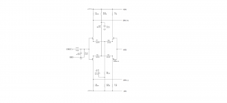
I am trying to build the Krell KSA-50. Here's the schematic of the input stage.
I couldn't manage (2N6431/2N6433) complementary pairs but instead I bought some (BC337/BC327) complementary pairs, hoping to finish the project. As far as I know, the 'hfe' of the transistors in the input stage of an amplifier need to be matched.
I bought around 2 dozens of each transistors but the 'hfe' of the NPN is not matching exactly with that of the PNP's. The closest match for 'hfe' I got was '265' for NPN and '242' for PNP's. I know there is a risk of DC offset at the output if the gain 'beta' of the transistors are not matched.
Now, if I build this amp with the transistors that I got, how much offset should I
expect at the output? Is there a limit in how much the 'hfe' can vary? Also, is there any other way like shifting (collector and emitter) resistor values to minimize the DC offset?
Please help. I am making this project on a protoboard and it will be difficult to solder or desolder the parts. I am asking this because if there is a maximum risk of the amplifier not being able to work properly, I won't build the project. Thnx everyone in advance!!!!
Attachments
Last edited:
Now, if I build this amp with the transistors that I got, how much offset should I
expect at the output?
Don't worry. There is the offset adjustment and also a lot of NFB.
Using Vceo = 45 V transistors on +/-50 V is a bit inadvisable, just saying... Try maybe some KSC1845 + KSA992.
What you are interested in is effective input bias current.
The effect of Ib can be greatly reduced by matching DC resistance at both inputs and using a feedback topology that gives unity gain at DC (or alternatively, an input offset adjustment), plus dynamically by matching AC impedance. Gain mismatch in both pairs is basically a non-issue here due to a healhy amount of emitter degeneration.
It is calculated like this:
Ib = I_tail / 2 * (1/beta_npn - 1/beta_pnp)
This peculiar function has some peculiar consequences.
If we define r_beta = beta_npn / beta_pnp,
Ib = I_tail / (2 beta_npn) * (1 - r_beta)
IOW, Ib depends not only on relative beta matching but also on absolute beta at the given collector current.
Assuming your betas still apply at 1.8 mA, they would result in an effective Ib of -0.32 µA. It would not be much greater (-0.35 µA) with betas of 700 and 550.
(And just for the record, input current noise does not cancel the same but actually adds up power-wise since all 4 transistors generate shot noise independently. In that regard, you want beta as high as possible.)
Last edited:
Hfe is only one parameter affecting DC offset. There are also temperature differentials due to air currents etc. and Vbe usually has an influence on the offset too. Some high quality designs even fit covers or bind the LTP pairs together with copper bands or wire in order to stabilize offsets and bias current balance.
2N6431, 2N6433 are 300V rated parts which is plenty of Vceo margin for an indicated rail-to-rail supply voltage of 100V. However, BC327/337 are only rated at 45V, so think seriously about having some more safety margin than what you may have with those substitute transistors.
If you buy plastic type semis in quantity and on cut tape, you'll also have a much better chance of matching the LTPs. Perhaps KSC1845/KSA992 from On Semi (140V rated) can do the job better and a lot cheaper than those TO18 can types.
FWIW, the amplifier will probably work fine with little attention at all to matching parts, as I have proven to myself many times. If someone wants their amplifier to be electrically balanced in all possible ways, I'm happy to do what they want but not for free. As you find, matching bulk packed semis by hand is difficult, tedious and expensive on semis and labour. 'better to use the chips from the same wafer by buying your semis in cut tape form, where you get better yields of matches to within say, 5% which should be adequate for hFE.
Agreed. That's a nice aim....say, 5% which should be adequate for hFE.
That's 9.5% difference and still acceptable considering the design and the amount of feedback....The closest match for 'hfe' I got was '265' for NPN and '242' for PNP's...
As said, BC337/BC327 wouldn't be not my first choises.
Good point; LTP transistor pairs should definitely be thermally bonded (by that I mean per pair, so npn+npn and pnp+pnp separately).Hfe is only one parameter affecting DC offset. There are also temperature differentials due to air currents etc. and Vbe usually has an influence on the offset too. Some high quality designs even fit covers or bind the LTP pairs together with copper bands or wire in order to stabilize offsets and bias current balance.
Hfe is only one parameter affecting DC offset. There are also temperature differentials due to air currents etc. and Vbe usually has an influence on the offset too.
Also, if we are going down the path of "other effects that give you offset". There are many beyond the input transistors. Some systematic, some random.
From the picture in post 1:
Systematic: I.e. Off-set due to design choices
- R1 <> R2 and R9 <> R10. Therefore, VCE of each transistor in the diff-pair is not the same and you will get off-set. FIX: Set R1=R2 and R9=R10.
- Even if R1=R2 and R9=R10, I_QN1 <> I_QN2 since R1 has a the current of the VAS injected into it and R2 does not. Same applies to the PNP diff-pair. The resulting offset will be (VAS_Input_current_P + VAS_Input_Current_N)/Combined_GM_of_diff_pairs = ~Combined_VAS_input_current * 100. FIX: Balance the GM loads by either a proper current mirror or a differential VAS.
NOTE: The transistors are not labelled, so I am calling QN1 and QN2 the transistors of the NPN diff-pair.
Random: Offset due to mismatch in components
- While, R7 =R8 and R5=R6 in the picture, these will not match unless you pay 'beaucoup' money. Say you pay for 1% match and IT = ~4mA. You will get a max Vos = R7 * 1%*IT/2 = 200*0.01*2mA = 4mV per diff-pair... which can lead to an overall offset between 0mV and 8mV depending on how the two pairs match.
FIX: Not really a fix, but an improvement, reduce the value of R5-R7.
Right now you got other problems on top of input transistor match, so make sure you address those too.
Last edited:
Thanks everyone for the valuable infos. Also, I am planning to use current sources in each pairs and trying to make the supply voltage regulated. Will it bring any audible difference compared with the design that I have now?
I am actually sorry for the pic, but the supply rails should be +-40 volts. The place where I live makes it very difficult for me to get some of the good transistors like you guyz mentioned. We always get a small variety of TO-92 package transistors. 🙁
I actually wanted to use MPSA42/92 pairs but it seems that high Vceo devices usually have low beta values and their 'hfe' values differ by around 50% for both NPN and PNP's. I've heard that high beta values are always efficient for small signal stages.
Please correct me if am wrong.
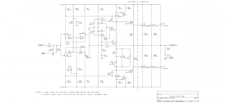
Below is the original diagram that am working on. I found it in the service manual of Krell KSA-50.
I am actually sorry for the pic, but the supply rails should be +-40 volts. The place where I live makes it very difficult for me to get some of the good transistors like you guyz mentioned. We always get a small variety of TO-92 package transistors. 🙁
I actually wanted to use MPSA42/92 pairs but it seems that high Vceo devices usually have low beta values and their 'hfe' values differ by around 50% for both NPN and PNP's. I've heard that high beta values are always efficient for small signal stages.
Please correct me if am wrong.
Below is the original diagram that am working on. I found it in the service manual of Krell KSA-50.
Attachments
Last edited:
Well, what types can you get then? Strictly speaking, none of us are spoiled for choice in terms of TO-92s these days. What other subs are you planning to use? It's not like it gets any easier for the VAS transistors.
BC337/327 are not too great a choice for input transistors - their Cob barely ever dips below 4 pF, and I think their Early voltage is very low, too. If you must use 45 V parts, at least get some BC550C/BC560C. And install some low-voltage zeners back-to-back in parallel with C3, just in case anything ever goes wrong.
One possible solution for the Vceo vs. hFE/beta dilemma: Use cascoding to take up some voltage, or even a lot of it (the cascode transistor is not nearly as critical in terms of beta, it should have high Early voltage and low Cob though). Maybe even a bootstrapped cascode, though this rather heavily degenerated input stage with its low gain is not overly affected by Miller effect as-is.
Current sources should help with power supply rejection and further reduce common-mode nonlinearity.
The downside to all this - circuit complexity has just increased quite a bit.
- Home
- Amplifiers
- Solid State
- Complementary LTP transistor matching