The common problem of using CMOS switches in analog/ low THD circuits is that there is parasitic variation of Rds, that directly leads to distortion. I'm thinking, that bootstrapping complete quad SPST switch like DG201B could potentially solved an issue. Am I missing something? Was it done before and published somewhere?
Attachments
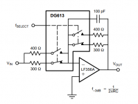
i saw an app note many years ago that used one analog switch in the feedback leg to cancel resistance modulation, kinda similar to the attached image, just so you can see in principal what I meant (note this app is a filter, though).
mlloyd1
mlloyd1
Attachments
Your circuits seems tracking R-ds On vs temperature, improving gain accuracy over temperature range. It points me that my example is also not the best, I could flip switches matrix and cancel common mode voltage, keeping everything at "virtual ground".
Question in this topic is to discus approach in general, for inverting and non-inverting topology, or in absence of virtual ground
Regarding negative feedback, there is app note from TI
https://www.google.com/url?sa=t&rct.../lit/slyt612&usg=AOvVaw0c9sir7RIa7nxoVaFEK2I0
Problem is that each switch demands it's own OPA, and good quality OPA is expensive.
Attachments

Yes, as you found out by yourself: in general, it is better to reformulate a problem rather than tackling it frontally, but there are (rare) cases where there is no other option, in which case your solution could work.It points me that my example is also not the best, I could flip switches matrix and cancel common mode voltage, keeping everything at "virtual ground".
It is severely restricted, because you can only bootstrap one node at a time in one entire chip, and it has to be the right one, and it adds some layers of complication to avoid injecting unwanted things into unwanted nodes through the substrate capacitances, plus messing up supplies and CM range, especially during startup.
All things manageable if you really need it, but that will probably be rare.
For example, adding a buffer to eliminate resistance issues will generally be OK, and simpler than bootstrapping.
That said, any addition to the "engineer's toolbox" is welcome, and could be useful to some people at one time or another, which is why I mark your idea as

Last edited:
Insert series resistor whose value is N times greater than switch on resistance --> reduce distortion by a factor of N.
Connect a number K of switches in parallel --> reduce distortion by another factor of K.
Connect a number K of switches in parallel --> reduce distortion by another factor of K.
Yes, as you found out by yourself: in general, it is better to reformulate a problem rather than tackling it frontally, but there are (rare) cases where there is no other option, in which case your solution could work.
Not exactly, there are cases where common mode voltage is unavoidable.
I'm getting at "variable resistor" cases, in filters, equalizers, oscillators etc.
Basically, only simple "input selector" make it possible to use inverting circuits
and get away with R-ds variation issue. Anything else - vast majority of electronics
- and analog switches are "not welcome" due to high level of distortion.
Now the problem is solved.
It is severely restricted, because you can only bootstrap one node at a time in one entire chip, and it has to be the right one, and it adds some layers of complication to avoid injecting unwanted things into unwanted nodes through the substrate capacitances, plus messing up supplies and CM range, especially during startup.
All things manageable if you really need it, but that will probably be rare.
For example, adding a buffer to eliminate resistance issues will generally be OK, and simpler than bootstrapping.
First, analog switches make it possible to adjust resistance,
16 combination out of one quad spst IC.
Another advantage of bootstrapping, is that no need to buy pricey low R-ds switches.
You can use any "ugly" 125 OHm and higher, it is O"K!
Third, charge injection. I'd not comment , this picture (1) explains that issue nulled out as well! Though initially I even was not aware, just a luck.
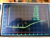
Today's proof of the concept tests. picture (2) Sanity signal source & SA test. picture (3)
(Don't know how to insert photo at this line, please read name of the pictures).
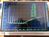
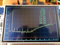
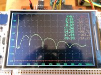
1. 16Vpp 3 kHz no load (100k).picture (4)
2. 16Vpp 3 kHz load (1k).picture (5)
3. 16Vpp 3 kHz load (1k) - bootsrapped.picture (6)
PS.
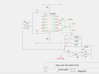
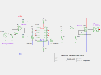
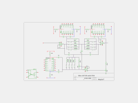
It bothered me quite for a whale that for simple adjustable Notch filter
I must use relay or mechanical switches. There is draft I gonna to try later on.
*schematic-picture (7)
Regarding
"Insert series resistor whose value is N times greater than switch on
resistance --> reduce distortion by a factor of N.
Connect a number K of switches in parallel --> reduce distortion by
another factor of K. "
Nothing of the kind.
1. Number K is a cost, not an option. Tween-T for example already has 2 OPA, all it takes is add one more and only to avoid loading of input source. Though, bootstrapping may also drive cost up, but not necessarily.
2. Resistor value is also not a solution, see tests results for 100k load. Bandwidth with 35 pF "Channel On" capacitance (page 3 datasheet DG413) 45 kHz.
Attachments
-
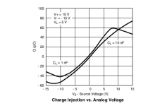 DG413-charge injection.png24.4 KB · Views: 204
 -
 dg413-1k-16Vpp-bootstrapped2.JPG868.6 KB · Views: 112
 -
 dg413-1k-16Vpp-a2.JPG966.7 KB · Views: 126
 -
 dg413-100k-16Vppx.JPG863.4 KB · Views: 119
 -
 behringer-uca222x.JPG942.7 KB · Views: 147
 -
 Ultra-Low-THD-Switch-test.png30.5 KB · Views: 201
 -
 Ultra-Low-THD-Switch-Tween-T-Notch.png63.1 KB · Views: 304
It depends on your definition of unavoidable: if you take some textbook circuit and translate it directly into an electronic version by replacing physical contacts with FET or MOS switches, you will indeed find many cases where it is unavoidable.Not exactly, there are cases where common mode voltage is unavoidable.
If you use some ingenuity in the topology, most of the unavoidable cases will become avoidable.
An example is your circuit:
Two of the groups are tied to a low-impedance node (opamp output), meaning buffers can work.
One group remains "unavoidable" with elementary measures, but it might also be solved with deeper topology alterations.
There will always be instances where the only solution is a mechanical switch or your bootstrap method, but I expect they will be rare.
You have developed a novel and useful tool, and I congratulate you for that, and I perfectly understand you are eager to use it, but remember: when your only (or preferred) tool is a hammer then every problem looks like a nail

The commonly used techniques in practice are
1) Use very low on-resistance analog switch, compared to the load impedance.
2) Buffer the output (ie draw no current through the switch, make the load impedance infinite)
3) Pass the signal through the switch as a current, not a voltage, at virtual ground. The resistance modulation no longer is an issue.
- Home
- Design & Build
- Equipment & Tools
- Nulling out Rds modulation of CMOS switch.