I have been around for a while in these forums, but haven't engaged to much in this forum, although it is fascinating hopefully one day I can catch up and actively take part. I thought ill introduce myself to break the ice, I am into DIY speakers and trying to learn more about amplifiers, PCB borads and so on.... Hence this basic question on a cheap bluetooth PCB board.
In the picture attached, the R3 is burnt out which correlates to only one channel working. The R3 is at the entrance of one of the channels so it makes sense why only one channel is working.
Is there any way to know what the part is, so I can find it and solder it in. I know the bluetooth is cheap but if its fixable then I am happy to attempt it.
And where can I get the part from if its identifiable?
Regards
Attachments
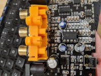
I suspect the R3 marking relates to the resistor near the IC as I can make out a C marking as well under the socket. That 3 legged part (that is the one you are referring to?) could be a transistor of some sort or perhaps a diode. Is there any ID under the socket?
When parts burn up like that it usually means significant current has flowed and so the question has to be asked as to what caused it in the first place. If it is a protection device then it may have failed due to some unsuitable voltage being applied to the input sockets.
Compare the reading (diode check etc) with the one next to it and see if you can identify what it is.
You could also try removing it completely and seeing if the stage now works.
Yeah, R19 and R26 should be similar in value to R3 & R4. Probe around with the DVM ohms scale.
In band equipment such burnout by the input is usually because somebody plugged a hot 75W guitar amp into an input. Inputs are for line level, 1.6 vac at 600 ohms source impedance. Maybe 2 vac is okay. Not an 8 ohm speaker driver output.
Source of free resistors is other broken equipment. You may need $12 of solder paste to effectively solder one in however.
I have no idea how it burnt out when it was sent brand new. Yes, the 3 legged tiny chip is the one I am referring to.
No ID, but I think its a transistor and on it, it reads "FB" if that helps. On top of the R3 it says, QI and C20....
So by finding its value with an Ohm meter I can find a similar transistor in other equipment? Any chance I can purchase it somewhere?
And one more thing is it possible to re solder it, as it is very small?
Hello Trdat,
to put some more detail, and (if I may) to help you learn:
in surface mount, often the markings are put "where there is space", and not ncessarily close to the component. The area with the markings reproduces the positions of the components (see my green additions in the picture).
So based on what you say, the burnt device (you said it's the 3-pin thing) would be called QI (maybe Q1?).
Q is a usual prefix for transistors, a diode would be D. The C20 and R3 are as I drew in red (the R thing has the looks of a resistor, and the C of a capacitor).
A transistor in this position it is probably a switch;
maybe possible to replace by pulling some equivalent from a "donor board" (often cd or dvd players near the output plugs, like in your board - you'll have to check the pinout of a working transistor neighbour to the burnt one, and find one with the same pinout).
Soldering can be done, but the most difficult is to remove the old part without damaging the traces.
There are tutorials online, of course.
I managed to repair similar things by gently lifting the component with a needle, while heating one pin at the time with the soldering iron.
To pull from the donor board, a hot air blower will detach many smd components at once.
_
Attachments

Last edited:
It is possible to remove it with an ordinary iron. Heat the single pin and lift/crack the device away from the board, then heat the two remaining pins together and again, lift/crack from the board.
Beware... if you are not experienced in this then it is easy to lift and damage the print below.
If this is a brand new unit then I would push for a replacement from the seller or company involved.
Beware... if you are not experienced in this then it is easy to lift and damage the print below.
If this is a brand new unit then I would push for a replacement from the seller or company involved.
Yes sorry, thought R3 must be a resistor. 3 pin devices are usually transistors. you might measure one in a similar posistion to see if it is npn or pnp. The pin that has the 400 to 700 mv drop on diode scale to the other two pins is base. plus from base to E & C is npn. minus is pnp.
Best thing if it is under 31 days is ask to return it for refund. If you broke a QA seal taking the case off you violated the warrenty.
Best thing if it is under 31 days is ask to return it for refund. If you broke a QA seal taking the case off you violated the warrenty.
So based on what you say, the burnt device (you said it's the 3-pin thing) would be called QI (maybe Q1?).
Q is a usual prefix for transistors, a diode would be D. The C20 and R3 are as I drew in red (the R thing has the looks of a resistor, and the C of a capacitor).
This teaches me a lot, thank you for your effort. Now that you have mentioned the above it is written in order above the 3 you coloured in the photo (although you can't see in the photo as it is underneath the RCA terminal)Q1 then C20 and R3 and it correlates to the order of teh capacitor and resistor that you outlined. So it is definitely a transistor.
A transistor in this position it is probably a switch;
maybe possible to replace by pulling some equivalent from a "donor board"
Yes, I will go to local electronic repair shop and see if they can help me out with finding one.
Soldering can be done, but the most difficult is to remove the old part without damaging the traces.
There are tutorials online, of course.
I was thinking this and realised it could be difficult but I will give it a shot.
I managed to repair similar things by gently lifting the component with a needle, while heating one pin at the time with the soldering iron.
So it is possible awesome thanks.
Appreciate it, I have learnt a lot about PCB boards from one thread.
FB = BFP17. It´s "through hole" equivalent is BFW92
I found the part with the number BFW92 in Mousser and Arrow but they are not available.
I will email to see if they have an equivalent.
This is especially helpful if on the off chance I don't find a donor board.
Yes sorry, thought R3 must be a resistor. 3 pin devices are usually transistors. you might measure one in a similar posistion to see if it is npn or pnp. The pin that has the 400 to 700 mv drop on diode scale to the other two pins is base. plus from base to E & C is npn. minus is pnp.
Best thing if it is under 31 days is ask to return it for refund. If you broke a QA seal taking the case off you violated the warrenty.
Mate the bluetooth is so cheap its probably not worth it but like I said I might possibly learn a lot just from this small burnt out transistor. So I am analysing all the posts above. I appreciate your comments....
Regarding warranty they have sent another one, but I am wondering if I can salvage this if possible.
I know, i said R3 and only later saw there was more codes above. The explanation by pilli clarified a lot more.
Looks like a dual schottky clamping diode. Very standard for input protection, clamps the incoming signal to within the power rails. If a large signal was present with the device powered down I might expect it to fry if the resistor before it wasn't large enough in value, since the signal is then trying to power up the board (phantom powering).
You can test this theory by seeing if two of its pins connect to each supply rail.
You can test this theory by seeing if two of its pins connect to each supply rail.
Looks like a dual schottky clamping diode. Very standard for input protection, clamps the incoming signal to within the power rails. If a large signal was present with the device powered down I might expect it to fry if the resistor before it wasn't large enough in value, since the signal is then trying to power up the board (phantom powering).
You can test this theory by seeing if two of its pins connect to each supply rail.
Hence:
You could also try removing it completely and seeing if the stage now works.
I also wonder (and it is really hard to tell with pictures) whether it is actually fried at all, or whether it is just a damaged part that has been placed during manufacture.
- Home
- Design & Build
- Parts
- Need Help with part on PCB board