Best to check at the output of the voltage regulators that drop the +15v down to 5v, and then down to 3.3v. If you don't know where to check, if you post a pic of the board you have we could probably point out where to probe.
If you have a scope or know someone who does, you could try checking the I2S signals and the dac clock to make sure everything is okay there.
Its possible you have a bad dac board. In that case, if the dac was purchased recently you might try contacting the seller to return it for repairs or replacement. Otherwise, you could try fixing it yourself, or maybe give up on it.
Then again, maybe someone else has some ideas of something else to try.
I just checked the output of both regulators and they were OK.
I think the problem is beyond both my equipment and expertise.
I bought the board over 18 months ago. While its too late to make a claim, I'll contact the seller and see if we can come to some arrangement for a replcement board.
Once again, thank you for your help
Naaling, my board works with jumpers on J1 and J2. I tried it with optical with my pc but it didn't work. Tv and dvd optical worked. The bitrate should appear in large number across the screen when its working even with IIS.
Are you sure the Amanero board is working and hooked up correctly? Try to start the up the dac with the IIS wires removed and see if the lights disappear.
Btw, you need to turn power on/off each time you change buffers or it will not respond.
Are you sure the Amanero board is working and hooked up correctly? Try to start the up the dac with the IIS wires removed and see if the lights disappear.
Btw, you need to turn power on/off each time you change buffers or it will not respond.
If a board works with both J1 and J2 installed it just means there is a different version of the firmware than most seem to have for board revision 1.07.
It should not be necessary to power cycle in order to change the dac input between I2S/SPDIF/TOSLINK, if that's what is meant by changing buffers?
However, if both lights are stuck on then power cycling is likely needed.
It should not be necessary to power cycle in order to change the dac input between I2S/SPDIF/TOSLINK, if that's what is meant by changing buffers?
However, if both lights are stuck on then power cycling is likely needed.
Last edited:
That pdf sorta answered my questions. Have did you tie dac earth with the op amps (for virtual grounds, not the AVCC op amp) middle voltage? (18V+, middle 0V, 18V-). In my solution they share the same ground layer and is tied. Is that the correct way of doing it? So all the earth symbols in multiple schematics refers to the same ground plane? In the picture one can see the new copper plate soldered on to the the old regulators ground..
Attachments
Last edited:
That pdf sorta answered my questions. Have did you tie dac earth with the op amps (for virtual grounds, not the AVCC op amp) middle voltage? (18V+, middle 0V, 18V-). In my solution they share the same ground layer and is tied. Is that the correct way of doing it? So all the earth symbols in multiple schematics refers to the same ground plane? In the picture one can see the new copper plate soldered on to the the old regulators ground..
There is only one ground potential for everything, no virtual grounds.
However, there is something we sometimes refer to as an 'offset-virtual-ground' which is at about +1.65v relative to actual ground. The name ESS uses for that sorta kinda offset virtual ground is Vref, and it is some fraction of AVCC, originally it was AVCC/2 = 1/2*AVCC. That's it.
Vref is only used by the non-inverting inputs of the I/V opamps, not for anything else.
Also, please don't confuse what we call the AVCC opamps with the I/V opamps. The AVCC opamps are used in our dac modding project as power supplies or voltage regulators to power AVCC, which actually is of two types: AVCC_L and AVCC_R. That means there are two AVCC opamps that supply 3.3v for each of the Left/Right dac channels.
The outputs of the AVCC opamps also power the Vref voltage dividers. There is one Vref voltage divider for each Left/Right dac channel.
Schematics for the recommended AVCC supply and for the output stage are attached to post #3003 of this thread. The Vref dividers are shown on the AVCC schematic. The output of those Vref dividers next appear on the output stage schematic and go to the non-inverting inputs of the I/V opamps.
Hope that explains it all this time 🙂
If not, sorry. I'm willing to try again if something still isn't clear.
Last edited:
Thanks, that made it a lot easier to understand. I noticed the feedback values are a lot different than the old schematic used early in this thread. I assume you use the ESS's values on feedback resistor of 2750ohm and the 100ohm resistor in series with 100pF cap in the feedback loop. Does these values sound better than the old scheme with 820ohm in parallel 330pF? My feedback loop uses the old values at the moment. Does the 2750ohm solution give more gain? I could use some more gain 🙂
The feedback resistor for the I/V stage is mostly what sets gain. You can increase the resistor value to increase gain, just don't make it too big or you could get clipping in the I/V and or the differential summing stage. 1.6k instead of 820-ohms might be within reason, but 820-ohms is enough to give around 3v peak to peak. That's somewhere around line level for most purposes.
The 2750-ohm value shown in the ESS document may have been for ES9008 or ES90018. Over time, Sabre dac output currents have tended to increase in order to improve signal to noise ratio. As dac output current goes up, I/V feedback resistors have to go down similarly to avoid clipping.
The 2750-ohm value shown in the ESS document may have been for ES9008 or ES90018. Over time, Sabre dac output currents have tended to increase in order to improve signal to noise ratio. As dac output current goes up, I/V feedback resistors have to go down similarly to avoid clipping.
Last edited:
Brilliant! I'll try some higher higher values resistors since the my old trusty Arcam gives out 6Vpp and both my amps are setup for that signal level. That explains my loudness problem^^.
Naaling, my board works with jumpers on J1 and J2. I tried it with optical with my pc but it didn't work. Tv and dvd optical worked. The bitrate should appear in large number across the screen when its working even with IIS.
Are you sure the Amanero board is working and hooked up correctly? Try to start the up the dac with the IIS wires removed and see if the lights disappear.
Btw, you need to turn power on/off each time you change buffers or it will not respond.
Hi Impuls60
Thank you for your reply. Unfortunately, I don't have the display, so I can't see the bitrate. As Mark suggests, there appears to be to be two different versions of the firmware for the 1.7 boards, and I can't be sure which one I have. My understanding is that all boards should be set up for I2S with both J1 and J2 open.
I have soldered pins to the DAC board, and use the same cable and connectors with both DACs, so I can see no reason why both shouldn't work. I have also tried switching the power on and off a few times to see if I can get the MCU to reset, without any luck.
The thing I don't understand is the source of the hiss. It only occurs when the Xmos board is connected. My Xmos board has provision for external power, so I connected it to the 5v outut on the DAC board. In this configuration, disconnecting the USB input has no effect on the hiss, indicating that it is not coming from the signal into the Xmos board but from the board itself. This is why I initially thought that the Xmos board was faulty. However it works without issue with my other DAC board.
Naaling,
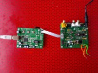
Could you post a clear picture showing the interconnections between your dac board and XMOS board? Maybe that would help us understand what is going on.
Also, if you just install J1 even though no TOSLINK input is present, do you still have both LEDs lit?
Could you post a clear picture showing the interconnections between your dac board and XMOS board? Maybe that would help us understand what is going on.
Also, if you just install J1 even though no TOSLINK input is present, do you still have both LEDs lit?
Naaling,
Could you post a clear picture showing the interconnections between your dac board and XMOS board? Maybe that would help us understand what is going on.
Also, if you just install J1 even though no TOSLINK input is present, do you still have both LEDs lit?
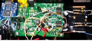
Some Photos
1. DAC powered by 12v wallwart. J1 and J2 open, with no inputs.
2. XMOS DAC connerction.
3. DAC powered by 12v wallwart. J1 open, with no inputs.
4. DAC powered by 12v wallwart. J2 open, with no inputs.
5. DAC powered by 12v wallwart. J1 and J2 shorted, with no inputs. (a bit pointless really!)
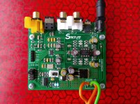

The first picture looks bad already. Did you try running it on +-15v rather than a wall wart?
What is the output voltage rating printed on the wall wart body? "15vdc, center +" ?
What is the output voltage rating printed on the wall wart body? "15vdc, center +" ?
I tested my dac with Amanero board and it couldn't detect the input without J1 and J2 connected at the same time. J1 alone, or J2 alone it failed to make a connection on 1.07 version.
The first picture looks bad already. Did you try running it on +-15v rather than a wall wart?
What is the output voltage rating printed on the wall wart body? "15vdc, center +" ?
Yes. I initially ran it on +-15v from 317/337 PS, with the same result.
The wall wart is 12vdc 1.5amp center+
Some Photos
1. DAC powered by 12v wallwart. J1 and J2 open, with no inputs.
2. XMOS DAC connerction.
3. DAC powered by 12v wallwart. J1 open, with no inputs.
4. DAC powered by 12v wallwart. J2 open, with no inputs.
5. DAC powered by 12v wallwart. J1 and J2 shorted, with no inputs. (a bit pointless really!)
Sorry that should have been
3. ............J1 shorted
4. ............J2 shorted
@Naaling : was the J6 short when you run +/-15?
No. It was open. I shorted the jumper when I switched to the wall wart.
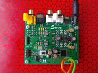
- Home
- Source & Line
- Digital Line Level
- ES9038Q2M Board