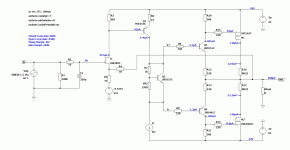
I have a question about assessing frequency response. As a learning exercise, I have been tinkering with singleton IPS CFA designs in LTSpice. The simplified attached schematic is inspired by Mooly's "MOSFET amplifier designed for music", Rod Elliott's P12 and Gareth's TGM8.
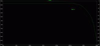
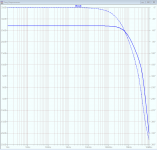
With C1 in place the frequency response looks good to me. However, when it is removed, I get a nearly 3 db hump in the response at 2.2 MHz. Is this an indicator of a potential stability issue? Adding a 33 pf Miller cap across the base and collector of Q1 solves this, but is it necessary?
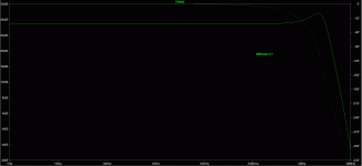
Other indicators of stability seem OK. Phase and gain margin look good and square wave response at 20Hz looks clean (with C1 in place... I get overshoot on the rise with C1 removed).
With C1 in place the frequency response looks good to me. However, when it is removed, I get a nearly 3 db hump in the response at 2.2 MHz. Is this an indicator of a potential stability issue? Adding a 33 pf Miller cap across the base and collector of Q1 solves this, but is it necessary?
Other indicators of stability seem OK. Phase and gain margin look good and square wave response at 20Hz looks clean (with C1 in place... I get overshoot on the rise with C1 removed).
Attachments
On the contrary of many think C1 is not RF filter . It grounds the gate at high frequencies so that the gate- source capacitance does not slow down the loop speed . By getting higher loop speed you get better stability.
R16&R17 must be on the sources not on the drains . The outputs not being voltage followers they don't need gate stoppers unless you need to driver-output feedback stability. The drivers are too weak , with more powerful ones you can drive the outputs by lower impedance, hence higher slew rate, faster driver-output response . I don't understand why with C1 you get -3db.
R16&R17 must be on the sources not on the drains . The outputs not being voltage followers they don't need gate stoppers unless you need to driver-output feedback stability. The drivers are too weak , with more powerful ones you can drive the outputs by lower impedance, hence higher slew rate, faster driver-output response . I don't understand why with C1 you get -3db.
I understand your reasoning for C1 to ground the gate for HF, never looked at it that way, interesting.
But seen from the source, it does attenuate the input signal through R1, so will also work in this way. After all, when you ground that gate you also keep the input signal from going to the gate, so the freq response will drop. 1k, 220pF about 800kHz roll-off?
Jan
But seen from the source, it does attenuate the input signal through R1, so will also work in this way. After all, when you ground that gate you also keep the input signal from going to the gate, so the freq response will drop. 1k, 220pF about 800kHz roll-off?
Jan
You want to be aware of the Miller capacitance of both BJTs and FETs, and don't go too far with base and gate "stoppers". The gate stoppers will cause a feedback lag that makes the CFP outputs unstable unless they are the dominant pole to begin with. Power MOS often have a ~1nF gate capacitance that requires a lot of current to charge and discharge, which is not going to happen with 2K ohms. Switching speed MOS requires gate drives around 10 Ohms and 1 Amp, but you shouldn't need to go that far.
I understand the attraction of using of these "lateral" FETs but you realize they saturate at like 12V so the most output you will get is about 30V out of a 42V power supply, ie lousy efficiency. Ironically, the "solves" the saturation issues of the CFP circuit by making it unattainable anyway.
I understand the attraction of using of these "lateral" FETs but you realize they saturate at like 12V so the most output you will get is about 30V out of a 42V power supply, ie lousy efficiency. Ironically, the "solves" the saturation issues of the CFP circuit by making it unattainable anyway.
Last edited:
I understand your reasoning for C1 to ground the gate for HF, never looked at it that way, interesting.
But seen from the source, it does attenuate the input signal through R1, so will also work in this way. After all, when you ground that gate you also keep the input signal from going to the gate, so the freq response will drop. 1k, 220pF about 800kHz roll-off?
Jan
Connect the bottom side of C1 to node In and you'll see whether the reduced overshoot was due to the filtering effect of C1 or the different impedance driving the input transistor.
No idea, it could be either or both. I should have phrased it differently, I used the term "you" in the sense of "one":
When one connects the bottom side of C1 to node In, one will see whether the reduced overshoot and/or peaking was due to the filtering effect of C1 or to the different impedance driving the input transistor.
When one connects the bottom side of C1 to node In, one will see whether the reduced overshoot and/or peaking was due to the filtering effect of C1 or to the different impedance driving the input transistor.
R16&R17 must be on the sources not on the drains . The outputs not being voltage followers they don't need gate stoppers unless you need to driver-output feedback stability. The drivers are too weak , with more powerful ones you can drive the outputs by lower impedance, hence higher slew rate, faster driver-output response .
The OPS stage is a CFP topology borrowed from Mooly's design. The only change was a slight change in the values of R14/R15. In practice the 2SK1056/2SJ162 pair would like be replaced by Exicon equivalents as these are no longer available.
No idea, it could be either or both. I should have phrased it differently, I used the term "you" in the sense of "one":
When one connects the bottom side of C1 to node In, one will see whether the reduced overshoot and/or peaking was due to the filtering effect of C1 or to the different impedance driving the input transistor.
Yes, I do understand the tactic. Hadn't thought about that one. ;-)
Jan
Simulation files attached.
Neither connection gives peaking. With C1 connected to Vin, fc is about 4MHz. With C1 to gnd, fc is about 500kHz. So C1 (with R1) seems only to provide hf roll-off of the input signal.
Jan
Attachments
I think I found the root cause. If R4/R5 are increased to 2700/127, the response flattens out. DC offset increases as a result, requiring the addition of a DC servo to compensate.
The value of 127 for R5 is just to maintain the same NFB ratio. In practice, this would be changed to 120 or 130.
The value of 127 for R5 is just to maintain the same NFB ratio. In practice, this would be changed to 120 or 130.
Neither connection gives peaking. With C1 connected to Vin, fc is about 4MHz. With C1 to gnd, fc is about 500kHz. So C1 (with R1) seems only to provide hf roll-off of the input signal.
Jan
I'd say it seems to provide HF roll-off and to improve the loop stability compared to the case when R1 is there but C1 is disconnected. Since C1 will always be there in practice and all other stability indicators are also OK, I don't think there is any small-signal stability issue at all.
A hump in the response isn't directly a stability issue, the phase margin and gain margins are, and they can depend on all the poles and zeroes. In general a big peak isn't good news though. High Q peaks are sensitive to component variation and add uncertainty to the response.
Adding passive components to swamp the device capacitances reduces the responses's sensitivity to the device variation (with load, temperature, individual devices and signal amplitude), at the expense of ultimate bandwidth - standard dominant pole Miller compensation is the classic example of this.
Adding passive components to swamp the device capacitances reduces the responses's sensitivity to the device variation (with load, temperature, individual devices and signal amplitude), at the expense of ultimate bandwidth - standard dominant pole Miller compensation is the classic example of this.
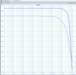
More musings on this... If I replace the output stage with a simple resistive load load, the hump disappears. That made think the OPS is loading the VAS at high frequencies.
Bob Cordell discusses this in chapter 4 and Chapter 13 in his new book. He describes adding a zobel network at the output of the VAS. If I add 100R / 2000p, the hump disappears (values are higher than what he recommends for a traditional miller compensated VAS).
This also preserves the low impedance NFB network that acts to reduce DC offset without the need for a servo (in theory). Under this topology, R4 would likely need to be implemented as four 0.5W to 0.75W devices in series parallel to cope with heat dissipation.
A hump in the response isn't directly a stability issue, the phase margin and gain margins are, and they can depend on all the poles and zeroes. In general a big peak isn't good news though. High Q peaks are sensitive to component variation and add uncertainty to the response.
Adding passive components to swamp the device capacitances reduces the responses's sensitivity to the device variation (with load, temperature, individual devices and signal amplitude), at the expense of ultimate bandwidth - standard dominant pole Miller compensation is the classic example of this.
+1
More musings on this... If I replace the output stage with a simple resistive load load, the hump disappears. That made think the OPS is loading the VAS at high frequencies.
I think what that means is that the OPS adds some phase shift to the signal, which is to be expected.
Jan
- Status
- This old topic is closed. If you want to reopen this topic, contact a moderator using the "Report Post" button.
- Home
- Amplifiers
- Solid State
- Frequency Response Question