希望看到完成版电路图和相关数据
 This is an English language forum. Please post in English or provide a translation.
I have provided a translation.
We want to see the complete version of the circuit diagram and related data
Further non English posts will not be passed.
Pay attention that this schematic has very poor PSRR. Even more - if no measures are taken it will amplify PSU noise.
With typical PSU (Rectifier and 10 000 - 40 000 uF capacitor's per channel) optimal results would be, when VAS transistors power supply is decoupled via RC filter lets say 20-50 Ohms and 4700-10000uF.
(in schematic R33 should be omitted, R28 = 20-50 Ohms, C9 = 4700-10000uF).
It will amplify psu noise, yes, but C9, R28 and R33 act as a buffer so it will at least be not as bad as it could be.
Imho too simple for real sq.
What do You mean "complete"?
With Power Supply (PSU) ? Or like this:
https://imampanggul.files.wordpress.com/2015/09/wpid-unnamed1.jpg
Can you provide a schematic that is complete and well labelled for us less technically gifted types that could be easily understood for a p-to-p build.
With Power Supply (PSU) ? Or like this:
https://imampanggul.files.wordpress.com/2015/09/wpid-unnamed1.jpg
It will amplify psu noise, yes, but C9, R28 and R33 act as a buffer so it will at least be not as bad as it could be.
Imho too simple for real sq.
What do You mean "sq"?
I think the best solution is to use here a capacitance multiplier, for two reasons:
1. Adequate PSU filtering with less capacitance.
2. Also acts as "soft start", less stress to the Power Transformer (especially toroidals has more stress because of very good primary to secondary coupling) initially charging all capacitors.
Drawback - some power is wasted, but in class AB it is not too much 🙂
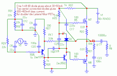
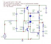
I had several questions regarding bootstrapped version, here is tested schematic with actual components. Performance is very good. I biased with Two diodes, got about 350mA. R20 and R21 - not needed - I used it only for testing purposes. Zobel network could be soldered directly at Output terminals - or at output capacitors PCB.
Attachments

Schematic: JLH, but simpler. PLH with bipolars. As example.
"Din" = noise. Awful noise;-)-; Just one complementary-parts-stage and you have got a sound like "spanish wall inside your (listening-)room"-)-;
"Din" = noise. Awful noise;-)-; Just one complementary-parts-stage and you have got a sound like "spanish wall inside your (listening-)room"-)-;
Schematic: JLH, but simpler. PLH with bipolars. As example.
"Din" = noise. Awful noise;-)-; Just one complementary-parts-stage and you have got a sound like "spanish wall inside your (listening-)room"-)-;
Yesterday I checked "Gainclone" with LM3875 (Output does not use complementary parts, it's "Quasi-complimentary") and this "My" amp (latest version, lets call it "v2.1") from noise perspective.
In "My v2.1" Amp I heard only very very silent hiss.
In "Gainclone" there is louder hiss (maybe because of the larger resistors in typical version), but despite that there is popcorn noise, or sometimes called "burst noise".
Burst noise - Wikipedia
And this noise is more Awful for me than silent hiss. Maybe I did not understand Your point?
First version is noisier than Gainclone - because of the large value resistors used in NF/signal path.
from where the 2sa1015 gets V+?
no current is flowing in the schema you posted?
Positive voltage 2sa1015 gets from output, here it is connected R17 from output to emitter. Positive voltage to 2sa1015 is equal about half of V+.
This is updated version of:
https://www.diyaudio.com/forums/solid-state/301486-simple-stable-power-amp-6.html#post5273712
More simple, but not worse.
https://www.diyaudio.com/forums/solid-state/301486-simple-stable-power-amp-6.html#post5273712
More simple, but not worse.
Attachments
My observations on the cost of simplicity:
20k input noise resistor = 2.6µV rms extra input noise (65µV at the output).
phase inverting
compensation using non-linear Cbc of Q1/Q2 - going to add significant distortion?
Do R20/R21 actually have a function with value that low? Why not lose them.
Gain mismatch in Q1/Q2 shows up as asymmetry in output voltage - probably should add a trimmer for that.
Output capacitor missing?
Q1's PSRR must be rather closer to 0dB than is desirable! And I think rail noise is going to directly modulate the VAS standing current. Adding some RC filtering to the supply to Q1 seems a great idea.
Q1 and Q2 would be destroyed if the rail was brought up super-fast (fortunately at normal rates of rise the base currents of Q1/Q2 would be tens of milliamps to charge the 22uF caps, but its risk to note when tinkering with the amp. RC filtering for Q1's supply can help here.
Last edited:
Ouch!!!! 😱
Do you realize speaker out has a DC component of 1/2 +V?
Do you now "this only works in simulation"?, where all parts same name are exactly the same?, no toleranceor spread involved, no offset, an ideal world?
That using actual physical parts top and bottom halves will NOT be symmetrical on any parameter?
And so on and on and on.
Although this will *seem* to work in a simulator.
Ouch!!!! 😱
Do you realize speaker out has a DC component of 1/2 +V?
Before comments like this - please read the topic "Single supply", and see the first schematic, the other link provided, description, and Yes Output Capacitor is obvious.
"Do you now "this only works in simulation"?, where all parts same name are exactly the same?"
Works not only in simulation... have you matched transistors h21E at least 10..15 percents and tested? I think no... but I did, so why are you writing so negative if You do not know? I have tested and written earlier how much offset I got...
Being familiar with analogue amp design it is obvious for me that this is quite a poor design. The flaws have been described above.
Being familiar with analogue amp design it is obvious for me that this is quite a poor design. The flaws have been described above.
Dear Voltwide, Please feel free to share Very simple and very stable power amp schematic with Push-Pull VAS, Source Followers current gain stage and Single Supply.
The internet is full of class-AB designs, there is no need to re-invent the wheel.Dear Voltwide, Please feel free to share Very simple and very stable power amp schematic with Push-Pull VAS, Source Followers current gain stage and Single Supply.
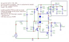
Regarding poor PSRR and Output capacitor -
Schematic was showed as principle only, here is more complete schematic.
Regarding Input Noise - Some expensive amplifiers have 50k (Or more) Volume Pot - at worse case it acts as 25k Input resistor.
Regarding Non linear Cbc - we need to use Cascode VAS or Emitter Followers before VAS - but I thing that is OK here because of a very Tight Negative feedback. Even in more complex schematics with Miller compensated VAS we sometimes get more distortion at High frequencies, because there is less Global Negative feedback left.
Attachments
- Status
- Not open for further replies.
- Home
- Amplifiers
- Solid State
- Very simple and very stable power AMP