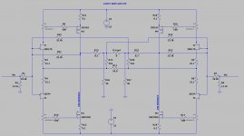
This schematic was posted by lhquam in another thread and it has intrigued me.
Each half was configured for only 1mV of DC offset before the halves were joined and the SUSY and PCF pieces were added.
The absolute output offset of was 260 mV before adding the 30 ohm resistors which lowers that to 230 mV.
My question is about the absolute offset. Would Zen Mod's Bablefish servo be of use here to deal with the offset?
I have all the semiconductors in hand to build this and want to plan for offsets and imbalances before committing the design to a PCB.
Attachments
Last edited:
if outputs are close to gnd potential (under 500mV) you're good
circuit is not the same as Aleph , so different servo would be needed
circuit is not the same as Aleph , so different servo would be needed
if outputs are close to gnd potential (under 500mV) you're good
circuit is not the same as Aleph , so different servo would be needed
Thanks
The next question would be how to bring it up the first time. The sims show that imbalances cause large large voltage offsets and large current hogging.
I did try F5 with laterals but it didn't work because of the low Vgs.
Will there be enough swing to drive the lats here ?
Figge
Will there be enough swing to drive the lats here ?
Figge
perfect reason to compare your LTSpicing with real world behavior
🙂
build it and bang it!
I have no doubt that it will work. My concern is that it will power up in berserker mode. There is one really good solution to the sim and 99 million berserker solutions.
My plan is to place some large resistances (several ohms) in the sources of the LATFETs where the sim has 0.1R to soak up large currents. After the imbalances are tweaked away, the resistors can be bypassed.
I did try F5 with laterals but it didn't work because of the low Vgs.
Will there be enough swing to drive the lats here ?
Figge
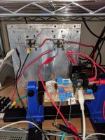
Last year, I built one channel on perfboard and it worked just fine. Attached is the picture. It is Nelson's simplified F7 circuit driving an IXYS hockey puck F4 beast OPS. The whole thing is still on a shelf staring at me every time I walk by.
Attachments
without load (8R) , what's minimum resistance output (halves) can see?
pretty much no berserking , except funny dc offsets , until you set it
I'm pretty sure that lhquam tried it , at least some iteration
pretty much no berserking , except funny dc offsets , until you set it
I'm pretty sure that lhquam tried it , at least some iteration
.without load (8R) , what's minimum resistance output (halves) can see?
pretty much no berserking , except funny dc offsets , until you set it
I'm pretty sure that lhquam tried it , at least some iteration
Yes I am concerned with DC offsets causing large bias current imbalances. With no load and a fault in one quadrant, the sim showed something between 4A and 6A bias in one of the LATFETs. I set the steady state no-load bias for around 1A in each of the 4 LATFETs.
After some adjusting in the sim, the absolute offset can be set to near zero with a slight bias current imbalance between N and P LATFETs.
The circuit is very sensitive to small adjustments. I can see that it may be a good idea to use a combination of a larger fixed resistor with a smaller pot once you know the final resistance values for steady state operation.
I'm tired , two cells functioning as 0,2 cells ..... but I can't see where is that path conducting 6A
path of least resistance is always 30R to gnd , so with rails of 23V , go figure ......
path of least resistance is always 30R to gnd , so with rails of 23V , go figure ......
I'm tired , two cells functioning as 0,2 cells ..... but I can't see where is that path conducting 6A
path of least resistance is always 30R to gnd , so with rails of 23V , go figure ......
I just pulled it up. In one of the sims, 4.6A DC has a path from +Vcc through J162 through the speaker through K1058 to -Vcc. It is a user error with the schematic somewhere but it shows me that a catastrophic fault in one quadrant can send 4.6A DC through the speaker.
Fortunately I have a nice collection of dummy resistors for the dummy constructor.
1. Power up without R24, R25 and load (speaker) and shorted input to set bias and offset.... Fortunately I have a nice collection of dummy resistors for the dummy constructor.
2. Connect R24 and R25, adjust offset, readjust after 30 min - 1 hour.
3. Connect large dummy resistor ~100 ohm, check bias and offset.
4. Replace dummy with ~ 8 ohm, recheck bias and offset, readjust after 30 min - 1 hour.
5. Test for stability with multiple types of dummy load.
6. Apply signal at input and observe at low power for several hours.
7. Repeat 6 at maximum power.
8. Replace dummy load with sacrificial speaker, observe for several hours.
9. If nothing dire happened, try with normal speaker.
1. Power up without R24, R25 and load (speaker) and shorted input to set bias and offset.
2. Connect R24 and R25, adjust offset, readjust after 30 min - 1 hour.
3. Connect large dummy resistor ~100 ohm, check bias and offset.
4. Replace dummy with ~ 8 ohm, recheck bias and offset, readjust after 30 min - 1 hour.
5. Test for stability with multiple types of dummy load.
6. Apply signal at input and observe at low power for several hours.
7. Repeat 6 at maximum power.
8. Replace dummy load with sacrificial speaker, observe for several hours.
9. If nothing dire happened, try with normal speaker.
Got it. Thanks. It makes sense. I just did a couple of sims and the circuit is less sensitive to imbalances with R24 and R25 changed to 1Meg.
I have never used Spice before and would not know how to sim this -
Q1: Does anything change if you substitute Exicon laterals in this circuit?
Q2: Which resistors would you replace with pots to adjust bias and offset
Q3: PCF and laterals - is this an X-ed F7 variant?
Q1: Does anything change if you substitute Exicon laterals in this circuit?
Q2: Which resistors would you replace with pots to adjust bias and offset
Q3: PCF and laterals - is this an X-ed F7 variant?
I have never used Spice before and would not know how to sim this -
Q1: Does anything change if you substitute Exicon laterals in this circuit?
Q2: Which resistors would you replace with pots to adjust bias and offset
Q3: PCF and laterals - is this an X-ed F7 variant?
Q1 Every individual transistor is different than every other individual transistor. You have to assume that some tweaking is involved when you build it no matter what LATFET is used.
Q2 Pots are in this circuit where bias and offset are adjusted, in the drains of the JFETs. You should read the entire "F7 review" thread and understand as much as you can.
Q3 It is exactly the circuit posted by lhquam in the F7 review thread. I did not link the thread in my first post. I did not invent it. I am evaluating it and planning for a build.
Right. Shame on me for asking questions. Maybe rename this thread to EE Rulez!
we are all entitled to have bad days right?
Thank you for the advice to re-read the F7 thread.
we are all entitled to have bad days right?
Thank you for the advice to re-read the F7 thread.
Right. Shame on me for asking questions. Maybe rename this thread to EE Rulez!
we are all entitled to have bad days right?
Thank you for the advice to re-read the F7 thread.
I had no intention to shame you. Is there a question that remains un-answered for you?
My apologies woofertester. I see the pots on the diagram now. Henceforth I shall refrain from trying to read these from my phone. This does look interesting and best of all doesnt require nearly extinct output devices. If I can manage to protoboard this I will be sure to post my experience.
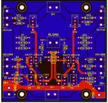
PCB en route
For whatever reason, this interests me more than making a standard version of the F7.
Test points were added so that every voltage at every node can be easily probed with a DMM or scope probe.
It will take a couple of weeks for these boards to get into my hands and some time to solder up the first one.
Last year I built one perf board F7 channel without the PCF and it was stable and behaved as expected so my stash of JFETs and LATFETs appear to be genuine.
Thanks again to Lynn for creating this config and to Nelson for his amazing talent and generosity.
Attachments
- Status
- Not open for further replies.
- Home
- Amplifiers
- Pass Labs
- LATFET SUSY with PCF