Um, no. Wire gauge doesn't actually determine how much current will go through a wire, just how hot it will get. A very short undersized wire will get enough heat-sinking from the wire around it to carry the current. It's the same way thermal reliefs on a PCB work.
Cheers,
Jeff.
Interesting.... thanks.
I suppose that must hold true also for the any vias on the PCB, where the current would have to flow through the via -- that via would also be of very small gauge, and need the wiring around it to act as heat sinking.
So, if that is of concern, then the wiring should try to not use the via, and wire from the other side.
Last edited:
It wouldn't be uncommon to insert a component lead into a via and solder in place.
But via's are rare on well designed boards...
But via's are rare on well designed boards...
Interesting.... thanks.
I suppose that must hold true also for the any vias on the PCB, where the current would have to flow through the via -- that via would also be of very small gauge, and need the wiring around it to act as heat sinking.
So, if that is of concern, then the wiring should try to not use the via, and wire from the other side.
I do subscribe to "avoid vias where possible", at least for the audio circuits (I don't worry about them in front-panel logic, relay control circuits, etc.).
When I do have to resort to one in a current-carrying situation, I reason it thusly: the circumference of the via is pi * D, so the un-rolled "tube" is roughly 3 times as wide as the hole. However, there's no copper foil under the tube plating (unlike tracks on the board surface), so it's 1/2 as thick. Therefore the via hole diameter should be about 2/3 the track width.
Note that even then the soldered-in stub wire can still a good idea to prevent failure due to differential expansion between the via tube and the PCB substrate.
It wouldn't be uncommon to insert a component lead into a via and solder in place.
But via's are rare on well designed boards...
Their use can be avoided here by wiring to the trace side of the board, as opposed to through the solder pad.
----------
On an unrelated note:
I have some heatsinks for solid state relays that have slight channels in them that don't allow the MOSfets/diodes to sit flat.... they're more than a few mm off.
Is it better to cut the boards in half or extend the MOSfets/Diodes?
Nobody?
You can, but you'll need to adjust values of either the drain or source resistors to get similar Vgs as the -BL versions.
Your overall OLG will change slightly as a result. In practice I find a single pair of -V a better option than two pairs of -BL when trying to drive (for example) three output pairs. The higher gain of the output stage more than makes up for the slight lowering of input stage gm, and if get the bias high enough it can sound pretty good.
Thank you! I'll order V-versions. Have huge heatsinks (~15kg each), don't need V3 turbo though, so F5"c" would suit me best with max 50w@8ohm and high bias for low impedance loads built as a monoblocks.
F5c pcb's are not around anymore, two turbo pcb sets from diyaudiostore would be overkill. Maybe normal F5 pcb's with wired cascode output..I don't know.
Edit; ordered two matched pairs from alweit.
Last edited:
... Is it better to cut the boards in half or extend the MOSfets/Diodes?
I extended the legs of the Lovoltechs in my F3 build:
The heatsinks have a vertical channel in the middle. There would be two per side, and that channel spacing won't fit the device spacing on the PCB.
I think Similar to what you've shown is the best way.... add two bars or a larger metal plate across the heatsinks upon which the MOSfets and Diodes are mounted. I did that on a Hotrodded DCB1 but totally forgot about it...
Darn good idea! THANKS!
I think Similar to what you've shown is the best way.... add two bars or a larger metal plate across the heatsinks upon which the MOSfets and Diodes are mounted. I did that on a Hotrodded DCB1 but totally forgot about it...
Darn good idea! THANKS!
Firing up F5T V2
Hi all,
actually firing up a F5T V3, 45V rails (33V secondaries), 2SK1530/2SJ201 Output, cascoded frontend as per ZM instructions, 1mA on R25/R27 (13Vish on the jfets) , 2 x 0.470R source resistors in //, bias set at 100mV across 0.235R, cooking for 1 hour know - pretty stable.
Is the 30W per output device still assumed the max ? That would be around 0.65A per Output transistor - giving me +/-150mV across the source resistors ?
Ohm's law is like a perpetum mobile to me - could someone kindly do a sanity check on my numbers ?
Thanks,
Max
Last edited:
Hi all,
actually firing up a F5T V3, 45V rails (33V secondaries), 2SK1530/2SJ201 Output, cascoded frontend as per ZM instructions, 1mA on R25/R27 (13Vish on the jfets) , 2 x 0.470R source resistors in //, bias set at 100mV across 0.235R, cooking for 1 hour know - pretty stable.
Is the 30W per output device still assumed the max ? That would be around 0.65A per Output transistor - giving me +/-150mV across the source resistors ?
Ohm's law is like a perpetum mobile to me - could someone kindly do a sanity check on my numbers ?
Thanks,
Max
Numbers look right to me. Max output will depend on the capacity of your heatsinks to dissipate the heat- 25C above ambient is target. What is it now?
nash
Yes, 150mV is around 0.64A per transistor, multiplied by 45 Volts is around 29 Watt per transistor. You are good, if your heatsinks hold the heat.
Congrats on finishing your amps. They will be very satisfying. Your numbers are good, check that the difference in temperature between heatsinks and room is around 25°C. I'll be higher if you push the bias current up. 25 degrees is a good safe number. Enjoy!
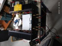
Without pics it never happened ...
Bias up to 130mV across 0.235R = 0.55A per pair if I'm not mistaken... still cooking...
Heatsink at +15°C vs. romm temp with 100mV, will cpost final figures -
WalterW, rembember those Seifert Heatsinks we talked about a couple of years ago.... I think I will limited by device dissipation rather than HS ..
Thanks to all,
Max
Attachments
Last edited:
Hi all,
actually firing up a F5T V3, 45V rails (33V secondaries), 2SK1530/2SJ201 Output, cascoded frontend as per ZM instructions, 1mA on R25/R27 (13Vish on the jfets) , 2 x 0.470R source resistors in //, bias set at 100mV across 0.235R, cooking for 1 hour know - pretty stable.
Is the 30W per output device still assumed the max ? That would be around 0.65A per Output transistor - giving me +/-150mV across the source resistors ?
Ohm's law is like a perpetum mobile to me - could someone kindly do a sanity check on my numbers ?
Thanks,
Max
Here is a thought, I may be wrong.
Your amp is a stereo version of the V3, your are using diodes in parallel with the source resistors.
According to Nelson's explanation of the design the diodes will start to conduct around 0.4 on the source resistors dropping the output impedance by a lot, delivering high current to speakers during transients.
I'll take 1.7 amps through the source resistors to produce 0.4 voltage drop to engage the diodes. But that bias current will be too high for the output devices.
Am I wrong? Why did you choose .47R as source resistors?
Here is a thought, I may be wrong.
Your amp is a stereo version of the V3, your are using diodes in parallel with the source resistors.
According to Nelson's explanation of the design the diodes will start to conduct around 0.4 on the source resistors dropping the output impedance by a lot, delivering high current to speakers during transients.
I'll take 1.7 amps through the source resistors to produce 0.4 voltage drop to engage the diodes. But that bias current will be too high for the output devices.
Am I wrong? Why did you choose .47R as source resistors?
Keremito, your are absolutely right. I am pretty sure that my diodes will never conduct... Problem is I started planning the project almost 5 years ago as 2 x V3 monoblocks.
That said your are right in my book! Being a fraidy cat as NP says even with 1R in // I would have been around 0.3V across them and closer to Nelsons indication. If I remember correctly I followed WalterW advise on the source resistors (lower them) because of the lower VGS of the Outputs... but now that you say it maybe I should replace them ....
Let me get my head around it....
Cheers,
Max
EDIT: If Papa says the fraidy cats leave the voltage drop at 0.3V does that implicate the diodes will never conduct ? Or does it mean only on higher transients ?
Last edited:
Bear in mind that NP says that the V2/3 really starts to sound better when the diodes are conducting. In my system, with nominal 4 ohm voltage, that is around 1 watt:
P = i^2 * R = 0.5^2*4 = 0.25*4 = 1
V = I*R = 0.5*4 = 2 Volts.
This will drive my speakers to 93 dB, which I find too loud for regular listening.
This implies that the F5T would be a better match with less efficient speakers and/or a much larger room, as the diodes would be conducting at normal listening levels.
The diodes are designed in to the circuit to conduct when the output current x Rs voltage drop rises high enough to forward bias them. The conduction voltage will change with temperature. You need to make certain that the diodes will never conduct at the no signal bias point. If they do it will probably lead to thermal runaway and release of the magic smoke from your mosfets.
I left the diodes out of my V3 monoblock build. There is not a huge power increase with a V3 unless you are driving really low impedances. It makes more difference with fewer pairs of outputs.
I left the diodes out of my V3 monoblock build. There is not a huge power increase with a V3 unless you are driving really low impedances. It makes more difference with fewer pairs of outputs.
- Home
- Amplifiers
- Pass Labs
- F5 Turbo Builders Thread