I've just received a pair of these dual AD1862 (mono dac) kits from DIYINHK. (not with the Xmos board or dac chips). I was disappointed to find that they have not provided the correct capacitors for the dac's noise reduction feature and don't supply any documentation. There are 3 chips labelled DRC1 and DRC3 but I can't find out what they are and where the FIFO is. i was expecting better but they aren't an improvement on most Ebay sellers.
https://www.diyinhk.com/shop/audio-...sampling-nos-audio-dac-with-fifo-reclock.html
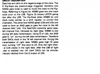
It seems to use AD's method (described on AN207) to convert I2S into the 3 wire PCM needed by the dac chips. (MSB first, left justfied, TWC) See image.
Their description is below and is slightly unusual in that both dacs receive left channel data which is transmitted first, then the left dac's clock is stopped so only the right one receives right channel data, then both dac's are latched at the same time. Reminds me of IanCanada's I2S to pcm board but for two's complement rather than offset binary.
I think the two of these boards will work with two TDA1541s - one board drives one dac with right & inverted right data, and the other drives the other dac with left & inverted left data. (with the TDA 1541s in TWC mode)
https://www.diyinhk.com/shop/audio-...sampling-nos-audio-dac-with-fifo-reclock.html
It seems to use AD's method (described on AN207) to convert I2S into the 3 wire PCM needed by the dac chips. (MSB first, left justfied, TWC) See image.
Their description is below and is slightly unusual in that both dacs receive left channel data which is transmitted first, then the left dac's clock is stopped so only the right one receives right channel data, then both dac's are latched at the same time. Reminds me of IanCanada's I2S to pcm board but for two's complement rather than offset binary.
I think the two of these boards will work with two TDA1541s - one board drives one dac with right & inverted right data, and the other drives the other dac with left & inverted left data. (with the TDA 1541s in TWC mode)
Attachments
Last edited:
I think the two of these boards will work with two TDA1541s
The TDA1541 is 16bit and the AD1862 is 20bit .
I've just received a pair of these dual AD1862 (mono dac) kits from DIYINHK. .......
What do you think of the quality of the board?
Despite the lack of documentation is there enough info to complete the build or are you going to return it?
What do you think of the quality of the board?
Despite the lack of documentation is there enough info to complete the build or are you going to return it?
When I enquired they said all the info was on the webpage but there is no mention the I2S input must be 3.3v, which is a serious omission given that most older CD players with I2S use 5v supplies.
The 3.3v input does not seem to be needed unless you buy it with the XMos USB board but again, I have had to ask the question and am waiting for a reply.
The boards and smd soldering is fine. The silk screen includes the pin designations but you need to consult the datasheet for the correct capacitors (1 and 10 or 2.2 & 22uf Tantalum - 2 of each per board needed.)
No excuse for not providing some basic documentation though.
I will only return it if it doesn't work - I'll find out in a few days.
The TDA1541 is 16bit and the AD1862 is 20bit .
Yes but my source is CD so 16bit.
When I enquired they said all the info was on the webpage but there is no mention the I2S input must be 3.3v, which is a serious omission ......
That's good to know. Hopefully the poor documentation isn't insurmountable. I'm very interested to follow your build and what you think of the sound quality. Thanks.
Yes but my source is CD so 16bit.
There is a bit more to it than that.
That's good to know. Hopefully the poor documentation isn't insurmountable. I'm very interested to follow your build and what you think of the sound quality. Thanks.
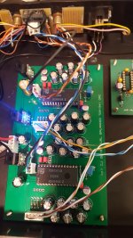
I am now listening to the DIYHK AD1862 NOS dac and it sounds great although its a while since my TDA1541 dac has worked so nothing to compare directly.
The stopping of the left channel dac does happen so both dacs are latched simultaneously as stated on their webpage.
I am using a SRC4192EV sample rate converter set to 20bit output and its on board SPDIF input (CS8414) from a Marantx CD65.
I have tried various output settings with FS of 22, 24, 48k and 48k is marginally better (bck is ~3Mhz with 48K FS).
Attachments

A further improvement is heard when increasing FS to 96K (bck = ~6Mhz, and mck = 12.88MHz). That's as high as the SRC will go from its SPDIF input.
I am now listening to the DIYHK AD1862 NOS dac and it sounds great ...
Well done!
Are there any problems with the build that would trip up a beginner?
Its cool having the SRC that puts out 20 bits for the AD1862. But my source puts only puts out I2S at 24bits. I wonder if you can please see if that works?
Well done!
Are there any problems with the build that would trip up a beginner?
Its cool having the SRC that puts out 20 bits for the AD1862. But my source puts only puts out I2S at 24bits. I wonder if you can please see if that works?
I've just tried all the output bit depths and heard no difference.
(96Khz Fs and 6.144mhz bck)
I am now listening to the DIYHK AD1862 NOS dac and it sounds great although its a while since my TDA1541 dac has worked so nothing to compare directly.
The stopping of the left channel dac does happen so both dacs are latched simultaneously as stated on their webpage.
I am using a SRC4192EV sample rate converter set to 20bit output and its on board SPDIF input (CS8414) from a Marantx CD65.
I have tried various output settings with FS of 22, 24, 48k and 48k is marginally better (bck is ~3Mhz with 48K FS).
Do you have a better photo of the I2S digital input section of the DAC PCB? I can see what looks like 2 regulators on the lhs near the I2s input, and 2 logic ICs and 2 other ICs on the rhs. Are they marked or has the seller rubbed that off?
I'm asking because I have just bought something similar and have yet to work out how the data is being processed. NOS DAC/I2S?? NOS????????I2S?????????-???
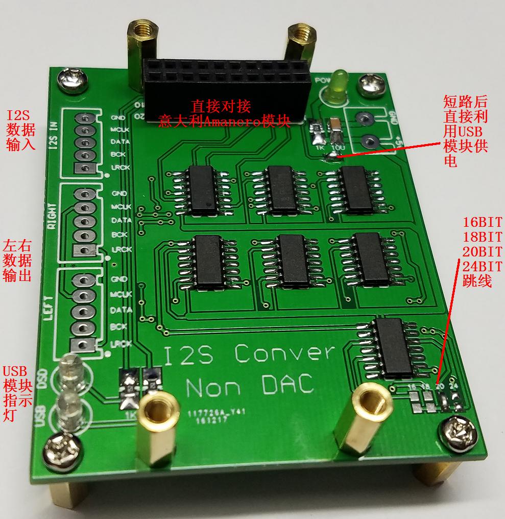
They are not the same.
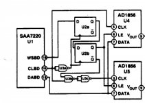
There are two chips labelled DRC1 & DCR3 which I can't identify and a LVC02 plus the 2 regulators. There are no jumpers to change any setting so it is effectively transparent to the incoming data which needs to be I2S.
The stop clock / simultaneous operation seems to be based on AD's application note. I posted a photo of it on an earlier reply, so the one of the DRC chips must be a flipflop and the larger one the fifo.
The signals to the dacs are 4.5v p-p which is presumably because the AD1862 is not reliable with 3.3v .
Attachments
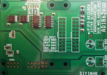
Ah, I thought the silkscreen must be marked DRC, didn't realise the seller had marked the ICs with it.
DIYINHK AD1862 Nos board update.
I have been listening to this for a few days and am liking the sound quality. Its a bit crisper than a TDA1541, and depth & imaging are very good.
Nor is it tiring to listen to and as you can see from the scope screen shot, the audio is clean. This is from the output of my Sowter Transformer with no other filtering whatsoever. (50r I/V resistor across the primaries), 20K Alps pot across the secondary.
The input is from the SRC4192EV sample rate converter using it's SPDIF input.
Output is I2S 20bit, 96K FS, 6.44Mhz BCK (so the SRC is upsampling from 44k to 96K which makes the transformer a more effective filter)
Next step is to connect the other one in parallel to boost the output.
Attachments

Last edited:
I've just tried all the output bit depths and heard no difference. (96Khz Fs and 6.144mhz bck)
Thanks for confirming the 1862 board processes 24bit data fine and also for posting up your photos and plot.
Is the standard IV on the AD1862 board just a resistor? It looked like the broad was designed for an opamp? Hows it sounding after a few more days?
Last edited:
Do you have a better photo of the I2S digital input section of the DAC PCB? I can see what looks like 2 regulators on the lhs near the I2s input, and 2 logic ICs and 2 other ICs on the rhs. Are they marked or has the seller rubbed that off?
I'm asking because I have just bought something similar and have yet to work out how the data is being processed. NOS DAC/I2S?? NOS????????I2S?????????-???
I just stumbled on this and find it very similar with the exception of another IC. Was thinking of using this on a TDA1541a under simultaneous mode but too ignorant to know whether this can function without MCLK since RPI I2S only outputs BCK, LRCLK, & SData.
Do you know if this can function as I2S to Simultaneous converter?
NOS DAC/I2S format NOS decoder shifter board I2S data conversion Right-Justified 926319274423 | eBay
Attachments

I just stumbled on this and find it very similar with the exception of another IC. Was thinking of using this on a TDA1541a under simultaneous mode but too ignorant to know whether this can function without MCLK since RPI I2S only outputs BCK, LRCLK, & SData.
Do you know if this can function as I2S to Simultaneous converter?
https://www.ebay.com/itm/NOS-DAC-I2...-conversion-Right-Justified/312050696208[/url
The AD1862 board can't be used with a TDA1541 because it does not convert the data into offset binary and does not stop both clocks. It also needs MCLK.
You need one of IanCanadas boards, I use his I2StoPCM board with dual 1541s in balanced configuration. It also stops the clocks once the 16bits have been received and converts the I2S data to offset binary which is required when using sim mode (pin 27 connected to -5v pin 26)
He does boards for the rpi and mclk input isn't always needed depending on which board(s) you choose.
[url]https://github.com/iancanada/DocumentDownload
Or contact Ryanj for his I2S to sim board (requires soldering)
DIY I2S to simultaneous converter PCB
The board in your link may work, but like so many Chinese boards, there is virtually no documentation which puts me off and it doesn't mention conversion to offset binary.
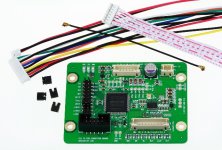
You may also be interested in my dual TDA1541 board. (bare board but no smd soldering unless you want ufl input connectors)
I will have an updated version available in January which will offer:
I am considering adding a ufl connector option for the 6 digital inputs.
The right hand photo is of IanCanada's I2S-PCM board. (it needs MCLK unless you use it with a FIFO & clock module)
There is no onboard I/V.
I will have an updated version available in January which will offer:
- TWC or simultaneous modes
- Can be used in parallel or balanced configuration (requires Ian Canada's I2S-PCM board for balanced)
- Uses ECDesigns low freq dem clocking (with their permission)
- Regulators moved to the board edges for easier heatsinking (where needed)
- Separate digital inputs for each dac. (to avoid routing digital tracks on the pcb)
I am considering adding a ufl connector option for the 6 digital inputs.
The right hand photo is of IanCanada's I2S-PCM board. (it needs MCLK unless you use it with a FIFO & clock module)
There is no onboard I/V.
Attachments
Last edited:
The AD1862 board can't be used with a TDA1541 because it does not convert the data into offset binary and does not stop both clocks. It also needs MCLK.
You need one of IanCanadas boards, I use his I2StoPCM board with dual 1541s in balanced configuration. It also stops the clocks once the 16bits have been received and converts the I2S data to offset binary which is required when using sim mode (pin 27 connected to -5v pin 26)
He does boards for the rpi and mclk input isn't always needed depending on which board(s) you choose.
GitHub - iancanada/DocumentDownload: Download documents of Ian's products
Or contact Ryanj for his I2S to sim board (requires soldering)
DIY I2S to simultaneous converter PCB
The board in your link may work, but like so many Chinese boards, there is virtually no documentation which puts me off and it doesn't mention conversion to offset binary.
Really appreciate your response, thank you Batteryman!
I had previously asked Ryan for his pcb gerbers to TRY and get started into analyzing how to on pcb design. Ryan graciously attached the gerbers - Thanks, Ryan!! But learning curve is a bit challenging. Hard to teach an old dog new tricks!
I will think about your suggestions, thanks again Batteryman.
- Status
- Not open for further replies.
- Home
- Source & Line
- Digital Line Level
- I2S to AD1862