Interesting what you have there Mike. Not sure I will ever go that way for one of my dacs, but I do like the cardboard box prototyping setup. Would probably put some tape on there somewhere to hold the transformers in place, you just in case anything gets jostled.
Looks like I may be joining you soon in playing around with an ES9028PRO, which I am primarily interested in doing to see how it differs from ES9038Q2M in terms of best possible sound quality. The only reason I can think of is the 256-tap interpolation filter option (if I can come up with some coefficients), and maybe more dynamic range associated with lower noise which in turn is is possible because of the higher output currents.
Anyway, my diyinhk board came today. It is only populated with the dac chip and an SMD voltage regulator for the 1.2v supply. I think I will have to replace the regulator with a 1.3v version though. That makes 1 mod lined up already.
Since the board is undocumented (they say the schematic is printed on the board - NOT), I spent the afternoon sketching out the schematic, and already thinking about the 2nd and 3rd mods. The second will be to redesign the output stage, and the third mod would be to try to bring out wiring to access the dac output channels they didn't use. They have two outputs in parallel going to each I/V converter, which uses up 4 out of the 8 total channels. They tied the other 4 channel outputs together in twos like they did with the first four channels, but they didn't bring out any traces from the dac chip big enough to solder to (by most reckoning). Maybe I will see if I can test out my microsoldering skills on those very tiny pins. Two sets of pins will be easy, and the last to sets of parallel pins will be hard as it gets, I think. Biggest problem will probably be getting the solder to go where I want it. The low temperature leaded solder I use tends to want to form bigger drops than I want, maybe due to surface tension when it is molten. We'll see.
I don't think that board will be suitable for the beginners. It looks intimidating.
Tape? Nah, I just lay it down and make sure the wires hold everything in place. Hence the fenced box to keep it together.
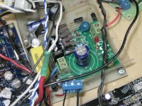
Tonite I forgot to attach a heat sink on the pass transistor for the power supply. Nearly burnt my finger when I wanted to see if I needed one.
Last edited:
Some might be wondering now. How does the PCM1794 with the Super reg sound compared to the Ebay 9028 board. They are close but the 9028 has less distortion and better bass control despite not having the ideal setup. When the Super Reg is transferred across, I don't expect it to be close. The DAC is destined for secondary use and for "pretesting" purposes like the canary in the coalmine. If I am going to smoke a dac, it better be cheap.
I don't think that board will be suitable for the beginners. It looks intimidating.
Oh, I don't know. I have the schematic now, and know what all the connections and jumpers are for. I could advise someone on how to get it put together and working.
However, it needs more power supplies than a Q2M, and by default it only works with I2S. There is no MCU, firmware, or volume control. Have to do all that stuff with an Arduino or whatever else is convenient. Not hard though. There are connection points provided to hook up I2C bus.
The board looks well made for 2-sided with pretty good ground plane coverage. Someone could just install the components (with parts values marked on the board), hook up power supplies and I2S source, and have a working dac probably similar in sound quality to an ESS evaluation board.
There is one thing I don't quite get though, it looks like they call out resistors to make Vref a little less than AVCC/2. Don't know what effect it would have on sound quality.
Things I don't think are good for a supplier of boards and kits that wants to be viewed as reputable is that not only is there no documentation, but the pictures in the diyinhk store don't show enough detail for anyone to have any idea of what they will be getting. Of course, the lack of documentation is standard for nearly all Chinese boards, kits, etc., sold on ebay or Aliexpress. However, at least some sellers do show more useful and informative pictures than diyinhk does. Doesn't seem very customer-centric to keep potential buyers in the dark.
These boards are really I think for the die hards who have an idea what they are getting into......let's say a year ago I would have stayed away possibly no definitely would NOT have a clue what I was looking at. Beginners beware kind of board I think and speaking of beginners.
Well there was quite a bit of experience gained today.
Well early on a Sunday morning I get up and decide what the heck, let me get going on this 9028pro dac. Maybe a couple hours and I can put in the Crystek clock, change the power supply to the Super Reg.
Well I took everything apart and then unsoldered the 5534 and then put in a socket. Then I grabbed my bank of ics. Took off the end clip and out slid an IC. The LME49710 I thought. Until I powered it up. 0.3 V huh. Looked over the circuit over and over and later out found out I slipped in an LME49720. Changed to a 49710 and the voltage was too low. 2.9V. Pulled it out. Put in a TL071 and again 2.7V. Put in three different 5534s and they all read 3.46V. Moral of story as I had learned 25+ years ago, these wide bandwith circuits and their layout are nearly matched to the IC model itself when designed to be stable. Op amp rolling in this is not recommended until someone tests it over many samples and variations and it is shown to be stable.
Next, I got down to installing the Crystek clock. The big gold TXCO chinese clock came off easily but I was expecting some landing below that on my board to tack on the crystek. Not on my version of board. I imagine the pictures I saw that this board had the landing was a later revision.
So I got down to figuring how to install the clock. Simple enough. I would tack on some wires on the bottom of the Crystek and then lead them back to the larger outline on the board. These clock thingies are small.
So I asked myself should I use some CAT5 wire of use of the silver plated teflon stuff. I elected on the latter as the teflon does not melt under the heat. This was some 20 gauge wire.
I got three legs on the Crystek easy enough but I had to use a very very fine soldering tip and note that Crystek has specific instructions on the heat range and duration when soldering these thingies.
The I started to fit the legs to fit the outline neatly before soldering it into place. I carefully bent the legs with a very fine pliers and got the first two fitting perfectly. Then I came to the third. It was a little off, so I elected to bend it with the other two in place and found a little wire had fallen off the clock.
The wire also held the landing on the Crystek. That leg was twisted off and there was no landing on the clock anymore. $30 clock down the "tubes". No I was going to fix it. I took out some large magnifiers and saw that there was still a sliver of metal on the side of the circuit board and a little on the top. But I had to remove the cover.
Then I got to see what's under the hood of a Crystek. Not much but all the stuff in there is tiny. So I figure out I made a mistake choosing solid core hard wire the first time. The small amount of metal to solder to on the side mandated I get as fine a wire as possible. Fortunately my parts bin still had tonearm wire I kept some 30+ years ago.
Tacked on a piece and elected to remove the other two solid core and use soft wires instead.
I got the clock put in and crossed my fingers that the clock was still good. Because of the soldering on the side, the cover on the Crystek had to stay off. I know that's not good but what else could I do?
Put everything together and fired up the system.
So the DAC in the state it in now is as follows.
The 9028PRO Ebay DAC.
IV Op amps OPA1612 and OPA1611 running buffer outputs.
IV Stage powered by Jung Super Regulators using the on board rectification stages.
AVCC supply, Sulzer Jung board running NE5534 using an LM385BZ-1.2V as a reference, prefiltered using an LM317.
Clock is a low jitter Crystek fed with the LT3042 preregulated with an LM317.
This is all fed from a Corcom RF filter feeding all the transformers.
I will post some pics of the current cobweb of wires later.
Still the last mods to come are a 3.3V AVCC powered by a Jung Super Regulator using an AD8031 and also using the LT6655 1.25V as a reference. The installation of an 80VA toroidal transformer feeding the Jung Super Reg.
As it sounds now....just super....the clock works!

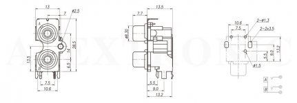
Searching doesn't really give me anything, so here goes: Has anyone made a mechanical drawing on the connector layout so I can make a Schaffer/FrontPanel Express panel for the original DAC board?
I guess they assume anyone buying that board will have sufficient technical prowess and skill to figure it out sans documentation! Certainly makes those wanting to customize it job easier. I hate desoldering components. Can make for a 'fugly' mess when it's all said and done. 🙂 Having a new, clean 'component-less' PCB helps. I really prefer a PCB with complete set of parts - mechanically designed for the board - even if it costs a bit more.Oh, I don't know. I have the schematic now, and know what all the connections and jumpers are for. I could advise someone on how to get it put together and working.
However, it needs more power supplies than a Q2M, and by default it only works with I2S. There is no MCU, firmware, or volume control. Have to do all that stuff with an Arduino or whatever else is convenient. Not hard though. There are connection points provided to hook up I2C bus.
The board looks well made for 2-sided with pretty good ground plane coverage. Someone could just install the components (with parts values marked on the board), hook up power supplies and I2S source, and have a working dac probably similar in sound quality to an ESS evaluation board.
There is one thing I don't quite get though, it looks like they call out resistors to make Vref a little less than AVCC/2. Don't know what effect it would have on sound quality.
Things I don't think are good for a supplier of boards and kits that wants to be viewed as reputable is that not only is there no documentation, but the pictures in the diyinhk store don't show enough detail for anyone to have any idea of what they will be getting. Of course, the lack of documentation is standard for nearly all Chinese boards, kits, etc., sold on ebay or Aliexpress. However, at least some sellers do show more useful and informative pictures than diyinhk does. Doesn't seem very customer-centric to keep potential buyers in the dark.
As it sounds now....just super....the clock works!
Wow, Mike. Sorry to hear you had so much trouble. I have written a few posts about replacing clocks including soldering the new one in. You could have posted a picture of the board with old clock removed and asked just kind of for a review of how to best proceed. But, the good news is you got it working despite some problems along the way! Good for you!
So, I trust the imaging has tightened up quite a bit with the new clock?
i would still suggest you better put an RC (some 10K/10uF) after those references.
Sulzer and Jung will enjoy that 🙂
The reason I was gung ho this morning is that last nite for bedtime reading, I reviewed the work that Walt Jung did in 1995 for high performance regulators and now I understand it much better but not all of it. It is quite some work that I can't imagine anyone should overlook. Based on what I see people doing now, it sure looks that that work has been overlooked.
Now regarding the noise aspect, remember these regs use LOTS of feedback and their topology is a lot more sophisticated than a unity gain op amp configuration.
Months ago, I could have linked the articles. Walt Jung has removed his web site now so I will extract a snippet of what was pointed out in his work. Hope he does not mind too much.
If you have access to the Audio Amateur series in Feb 1995, then you can read the complete article and others following up to 2000.
Walt Jung did some very impressive work indeed.
Attachments

Last edited:
Not that I know of yet. That can be one of the most time-consuming tasks of DIYing - at least to my standards anyway. I usually, grab my calipers and the board and start measuring. After I get close, I print the FP diagram panel out on paper. I then cut out the holes, see how the board fits and finesse the size and location in mm movements, and adjust the FP layout accordingly. Usually it takes several iterations before the final is locked down. It's a slow process, but I've gotten pretty good at it over the past several years. It can be an expense many don't bother with.Searching doesn't really give me anything, so here goes: Has anyone made a mechanical drawing on the connector layout so I can make a Schaffer/FrontPanel Express panel for the original DAC board?
Here's a couple of samples. Apologizes Mark, don't want to hijack the thread.
Attachments
Wow, Mike. Sorry to hear you had so much trouble. I have written a few posts about replacing clocks including soldering the new one in. You could have posted a picture of the board with old clock removed and asked just kind of for a review of how to best proceed. But, the good news is you got it working despite some problems along the way! Good for you!
So, I trust the imaging has tightened up quite a bit with the new clock?
Yes, the imaging has changed. The bass has tightened up a bit leaner. The biggest change was the voices now hang in the air. Now I don't know if this was the clock or the Super Reg.
Actually, the clock appears in this case to be more icing on the cake but not a crucial element IMO. AVCC and high speed regulation of the voltage is the most important part. Low noise for AVCC IMO is chasing the wrong parameter based on what I have experienced. Once the noise is low enough its fine....it is the wide bandwidth regulation that is needed. Again just my opinion.
One weakeness with the board you've got is the IV voltage section. If they went to the trouble to separate AVCC L&R, why not provide the potential to also separate the IV voltage rails. They could have put in four holes to allow jumpering to a single power supply.
Here's a good question. Since the board does not use a clock. That means that the clock is had from the circuit outputting IIS. So does that mean XMOS and Amanero boards control the clocking on the DAC?
You talking about your cheap dac board not having a clock? It clocks from XMOS board then. Some dacs may need the mclk signal in that case.
Regarding imaging, the clock tightens it up, the clock power supply adds icing on that. But, we do everything that helps because it all adds up. You can't get from good to great unless you go after all the little details.
For ES9028PRO, VCCA and the clock should be on a low noise regulator. They need better quality power than, and to be isolated from, the digital 3.3v power. However, they are not as critical as AVCC is.
EDIT: The reason for separating AVCC power into left and right, but not the output stage channels, is because AVCC has zero power supply noise rejection (PSRR). Any junk on the power adds to and intermodulates with whatever audio is coming out of the dac. That includes any small voltage variations caused by music playing in the other channel if both channels use the same AVCC supply. That's all bad. They need to be separate from each other even with the best AVCC supplies, because otherwise stereo separation suffers. The output stage is completely different. The opamps have pretty good PSRR, so there is no advantage to be gained from isolating their power between left and right.
Last edited:
Thanks. That's basically my approach as well, so if noone else has done it already then I looks like I have to get the calipers out and turn on the printer 😀Not that I know of yet. That can be one of the most time-consuming tasks of DIYing - at least to my standards anyway. I usually, grab my calipers and the board and start measuring. After I get close, I print the FP diagram panel out on paper. I then cut out the holes, see how the board fits and finesse the size and location in mm movements, and adjust the FP layout accordingly. Usually it takes several iterations before the final is locked down. It's a slow process, but I've gotten pretty good at it over the past several years. It can be an expense many don't bother with.
Maybe time for a little update on the dac project. Currently, I am finding that OPA1612 opamps in the output stage seem to be giving a more honest sound than LME49720 types. Perhaps that is due to some small amount of RF I have not been able to fully shield them from. A lot to artificial brightness is gone with the new opamps. Still have LME49720 on the AVCC board. Maybe will try a substitution there later, although I don't hear any indication of anything wrong.
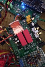
Where I am seeing the last bit of improvement I can get that brings the dac really close to not having a sound of its only, it just plays whatever is on the recording, comes from adjustment of DPLL bandwidth. It starts with a default value of, let's call it 10, and if I can get it down to 8 out of 10 that sounds a bit better, but I like definitely like it better if I can get it stable at 7. That turns out to be much tougher as stability seems to tend to drift with time and temperature. Some experiments show where the sensitive area on the board is as can be seen in the picture below. It is where the I2S signals come into the dac and and bit the right side of the big AVCC film caps. I found dropping a piece of copper foil in there with the backing still attached so as not to cause any shorts helped some. I was actually able to get DPLL down to 5 although I couldn't get it to stay stable for long. Where the copper foil is also happens to be where I can probe around with my finger to affect stability.
Last night I tried a new experiment which looks like it might offer more reliable stability of the EM fields in that area. I laid a small plastic bag of ferrite cores into the sensitive area. I would hoping they might be lossy at the sensitive frequencies or at least help keep the fields more well defined and contained to a very local area. Don't know exactly what is going on, but it seems to be helping. I will try to play around with it some more today to see if I can learn a bit more.
Attachments
Last edited:
Searching doesn't really give me anything, so here goes: Has anyone made a mechanical drawing on the connector layout so I can make a Schaffer/FrontPanel Express panel for the original DAC board?
I have some attachments that might help. That's about it though.
Attachments
Maybe time for a little update on the dac project. Currently, I am finding that OPA1612 opamps in the output stage seem to be giving a more honest sound than LME49720 types. Perhaps that is due to some small amount of RF I have not been able to fully shield them from. A lot to artificial brightness is gone with the new opamps. Still have LME49720 on the AVCC board. Maybe will try a substitution there later, although I don't hear any indication of anything wrong.
Where I am seeing the last bit of improvement I can get that brings the dac really close to not having a sound of its only, it just plays whatever is on the recording, comes from adjustment of DPLL bandwidth. It starts with a default value of, let's call it 10, and if I can get it down to 8 out of 10 that sounds a bit better, but I like definitely like it better if I can get it stable at 7. That turns out to be much tougher as stability seems to tend to drift with time and temperature. Some experiments show where the sensitive area on the board is as can be seen in the picture below. It is where the I2S signals come into the dac and and bit the right side of the big AVCC film caps. I found dropping a piece of copper foil in there with the backing still attached so as not to cause any shorts helped some. I was actually able to get DPLL down to 5 although I couldn't get it to stay stable for long. Where the copper foil is also happens to be where I can probe around with my finger to affect stability.
Last night I tried a new experiment which looks like it might offer more reliable stability of the EM fields in that area. I laid a small plastic bag of ferrite cores into the sensitive area. I would hoping they might be lossy at the sensitive frequencies or at least help keep the fields more well defined and contained to a very local area. Don't know exactly what is going on, but it seems to be helping. I will try to play around with it some more today to see if I can learn a bit more.
You might want to even try using an OPA1622 on the difference amps, the last leg. You should be able to drive your headphones adequately directly from that output. The last leg wants to see more drive current capability for some unknown reason. The OPA1622 is supposed to do that...however it is slightly lower bandwidth but decent considering what they are packing into the die.
It would be interesting to say the least and compare that to when an additional stage like your HPA is added.
OPA1622 DIP8 High Current Output Low Distortion Dual Op Amp | eBay
http://www.ti.com/lit/ds/symlink/opa1622.pdf
There's even a laser trimmed version that apparently offers up some real precision resistors built into the op amp for you to exploit for serious matching.
No way on the OPA1622. Its hard enough to find a good opamp that makes a good line output. Expecting one to do differential summing, filtering, and then also drive headphones would mean sound quality would suffer. And, couldn't use any built in resistors, they must be chosen to give the needed filter time constants for the output stage.
Anyway, for a headphone amp I would probably use LME49600. Think it makes a very good choice if the implementation is proper. Thanks for asking though.
Anyway, for a headphone amp I would probably use LME49600. Think it makes a very good choice if the implementation is proper. Thanks for asking though.
Last edited:
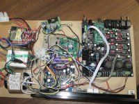
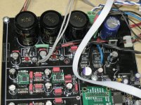
Here is my web of confusion.
Here is the rejigged Crystek on the bottom right hand corner WITHOUT the cover!
Just above it is the LT3042 that will eventually power it exclusively. I feel the constant power required is something the LT3042 was really meant for. We shall see.
Right now it is also powering other 3.3V requirements besides the clock. When the sampling frequency increases the power drawn increases and thus I had the need to increase the heatsink. When it goes back to powering the clock exclusively, the additional heatsinking will be removed.
Attachments
Last edited:
Yep. That looks to be pretty heavy gauge wire supporting it. I'm sure a lot of people would be interested to take a look at the insides of one. Good that you got it working. After that I would say you are probably getting increasingly qualified to work on small parts. If you can solder small enough little strands of wire, surprising some of the things you can fix.
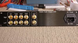
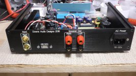
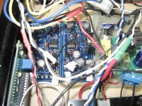
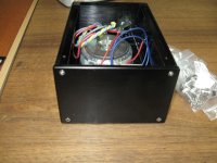
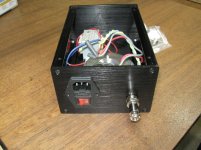
Here is the system as it is now.
The external power transformer cases will be finished first. Inside is an 80VA toroid for the IV stage , there will be a separate transformer to power 5V & Digital 3.3V, the AVCC and clock will likely share the same transforner. Depends on space left inside the enclosure.
Inside the DAC some tight packaging will be involved.
Attachments
- Home
- Source & Line
- Digital Line Level
- ES9038Q2M Board