They also go on to explain technically why they feel the OPA1612 is superior to the LME49723.
One needs to compare the specs of the LME49723 and LME49720 now and see if they are identical.
One needs to compare the specs of the LME49723 and LME49720 now and see if they are identical.
Last edited:
Hi Mikett, Thanks for the links to TI applications info, and of course for your enthusiasm.
To me the TI app note looks pretty basic. The optimized the design for measured performance probably without ever measuring distortion at more than one output level. My guess would be that the ESS recommended designs sound better with music and measure better over a wider range of output levels, especially with tougher distortion tests such for IMD.
My guess would also be that we might be able to do a little better than the ESS recommended designs if we do a little bit more filtering. Opamps can only filter effectively up so high, eventually their gain falls off and our assumptions about how they work become less accurate. For audio frequencies that should be negligible, but we likely have a little bit of RF we should be trying to filter out too. ESS would probably do more of that too, but their data sheets tend to indicate they test with clock frequencies at a minimum for playing back CDs and DVDs.
They seem to leave it up to the designer if they want to figure out how to best design circuitry for the dacs to run full out with 100MHz clocks, not that that is necessarily the best way to run them, but that's what we mostly seem to do.
Thx Mark, If the rising phase was assuming 1 ns (or slower) we need no care of the distance of the wire up to approx. 5 cm. Because of the purpose of the Signal Integrity , at the longer distance (or faster rising edge than 1 ns) at the output, assuming the output impedance of the 20 Ohm of the logical gate of the Crystek + 30 Ohm settig resistor, an 50 ohm coax cable is necessary.
Thank you for the update on the clock. Looks like a nice little board. Hope you won't mind if I say that with 100MHz RF, I always feel more comfortable if it is soldered to the dac board right next to the dac chip. But, if enough of the right care is taken, it is probably possible to get very nearly the same results with a clock a short distance away. Also, with the growing popularity of ufl connectors, I sometimes wonder that we still pipe around 100MHz RF on pin header connectors like it was only 10MHz.
Last edited:
Hi janos_904, That is an interesting point you raise. However, I'm not sure whether or not clock output loading impedance and transmission line theory are the only considerations. Even a short piece of wire can act like an antenna to some degree. Any vibration of the wire if it is not rigidly held in place can modulate local EM fields around the wire enough to increase jitter level at the receiver end. Someone else here recently reported problems with clock noise seen all over the dac board when using an external clock, although the exact physical construction was not given. Without looking into all the things that can happen the safest thing is probably to put the clock right on the ground plane right next to the dac, but a very short distance away might not be too bad, it is just very hard to say without seeing it and or simulating stray coupling around the clock output and ground return path with an EM code. Or, the old fashioned way to do it might be to wire it up then look at some adjacent dac circuitry with a fast scope while moving the clock board around a little. If no stray pickup then at least that part is good, also less likelihood of much jitter being induced. Anyway, hope it works well for you however you set it up. If you think we can learn something useful from the arrangement please post pics. 🙂
Last edited:
Hi bih, You have a lot of questions!
Thank you for your explanation. I think I have to do it step by step. First I start with a prototype on a wooden board and then I can try to improve all mods and compare them to my HUD-mx2 DAC.
If you can list the links to the mods, it would be helpful.
Hans-Peter
If you can list the links to the mods, it would be helpful.
Hi Hans-Peter,
I will post attach below the list I have now although it may be getting too long. Another thread has been started to help people too that you might want to look at. Sorry, maybe what we have at this point isn't quite ideal for people just starting.
Also, the other thread is here: ES9038Q2M Production
Attachments
A quick update on some current events:
*Ordered some parts to make through-hole output stage and AVCC. Maybe have parts later this week or early next. Think an output stage can probably go together pretty quickly once the parts are here.
*No word yet from Allo regarding shipment of Katana 1.2 boards. When they get here it probably won't take long for some initial findings to present. More of an official review may have to wait a bit longer. Hope to be able to describe Katana in terms of its sound quality, but also in terms of some of the things that make it technologically different from other ES9038Q2M dacs. Will try to make it interesting.
*While waiting for the above items, thinking about Serge's effort to make a modding tutorial verses my long list of links to old posts that has already gotten much too long. I am not sure that either of those newbie resources is doing the best job of being helpful. My list is too long, and not focused enough on newbie needs, and I hope Serge will not be offended if I say his documents could probably benefit from improved pic focus and lighting. Both resources probably aren't all that good if they keep going exactly like they are, so probably need to do something. Any help with that would be very welcome, of course. For my stuff I am kind of thinking about picking out the most informative pictures and descriptions and putting them into a new format of some kind. Doesn't have to be my stuff either, just whatever we have that can be helpful for getting people up to speed on what can be done and a suggested order for doing the most important stuff first. Maybe include some info on what not to do as well. 🙂
Hi occip,
Thank you for the update, lots of work there. Curiously, what is possible to do with custom XMOS firmware, is it volume only? (Assume you are aware that volume control in the ESS dac chips probably preserves more bit resolution than other digital volume controls, because it can be implemented in the upsampled modulator. http://www.esstech.com/files/3014/4095/4308/digital-vs-analog-volume-control.pdf)
Also, may I ask if you can hear any difference in sound quality between the two dacs you have been comparing?
Possibly tried AK4137 yet?
With Custom firmware you can do anything, DSP, ASRC , manage I2C peripherals. the xmos xu208 has 500MHz cpu so a lot of things can be implemented on the data path ( from USB to I2S)
When I said hardware volume I mean es9038q2m managed volume in opposite to software volume in Xmos firmware.
I have to do more listening session with the 2 DACs, maybe less bass on the Tone Board than my modded es9038q2m chinese board( big caps on the avcc ( plus the aop))
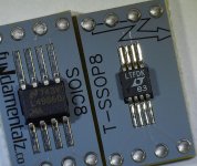
Wanted to show what would be involved in soldering an LT6655 precision, ultra low noise voltage reference to an adapter board for use as an AVCC reference. I would definitely recommend practicing with some SMD parts first just because LT6655 aren't cheap, maybe $7. Good news is it would only take one which could be shared by both AVCC channel opamps (one dual opamp).
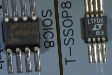
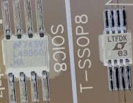
Will attach some pictures below showing that LT6655 is a bit smaller than things like typical dual opamp SMD parts. The opamp on the left side of the pictures is the same size as the IC that I made a video of soldering the other day.
An inverted picture is included and may help show the pins and solder pads more clearly.
The last pic is a close up with the solder iron tip on the right being the one I used in the IC soldering movie. The iron tip on the left is the smallest one I have and a bit tricky to use with leaded solder because the solder tends to get drawn away from the end of the tip by the hotter mid body of the tip.
Also shown is some 0.3mm solder for size reference.
The good thing about the better little SMD adapter boards is they are tinned enough so that traces are slightly rounded with a little extra solder. To solder an IC it is not necessary to add any additional solder. A very small iron tip like the one on the left can be placed in the end of a trace away from the IC. Then the tip is pushed towards the pin. It makes a little wave of solder ahead of it that is just exactly the right amount of solder for the pin. So, it's just a little push for each pin and you are done.
The most important thing about the whole process is to take as much time as it takes to get the IC aligned with the pads, and secured in place. That is the hardest part. The actual soldering is usually easy using a very small iron tip.
The other way I have found that works to solder small ICs is to use a bigger tip and solder all the pins on one side at once. Let it bridge a little, just don't add so much solder that it goes under the IC.
One should try to apply the solder to the outside half the pins and not get too close to the chip, at least as goal or strategy. Once the pins are soldered, just remove any bridges all at once with a piece of high quality solder wick and the flat side of the iron tip laid across a strip of wick. It will suck up any bridges.
If one examines the joints carefully there is enough solder under the pins to attach them to the traces, but only just enough. The skill involved at that point is with wicking so as not to remove more solder than is desired. If a good magnifier shows more solder is needed then more can always be added and then wicked off a bit as needed. It normally gets done in one or two tries, assuming one has practiced the technique first. Not hard though, just a little different the what we usually do.
Of course, it should go without saying that one needs to use some kind of temperature-controlled iron, solder than has been freshly wiped clean of oxides, best quality solder wick you can find (maybe Chemtronics), and a tip cleaner such as the brass wire pad type.
Attachments

Updates:
Remaining parts for through-hole output stage and AVCC expected this Friday. Guess I know what I will be doing this weekend. 🙂
No word on Katana 1.2 shipment yet, but still expecting news on it any day now.
Anyone else making any modding progress?
We are always interested to read the latest news from our dac modding folks as they move forward on their journeys.
It can be a whole lot to do, as most probably already know. For those that are still kind of new to all this, pictures of a fully modded dac less case can be seen here: http://www.diyaudio.com/forums/digital-line-level/314935-es9038q2m-board-229.html#post5515145
Sure looks a fair amount different from this:
US ES9038 Q2M DAC DSD Decoder Support IIS DSD 384KHz Coaxial Fiber DOP Fast Ship | eBay
Updates:
Remaining parts for through-hole output stage and AVCC expected this Friday. Guess I know what I will be doing this weekend. 🙂
No word on Katana 1.2 shipment yet, but still expecting news on it any day now.
Anyone else making any modding progress?
We are always interested to read the latest news from our dac modding folks as they move forward on their journeys.
It can be a whole lot to do, as most probably already know. For those that are still kind of new to all this, pictures of a fully modded dac less case can be seen here: http://www.diyaudio.com/forums/digital-line-level/314935-es9038q2m-board-229.html#post5515145
Sure looks a fair amount different from this:
US ES9038 Q2M DAC DSD Decoder Support IIS DSD 384KHz Coaxial Fiber DOP Fast Ship | eBay
Hello, do you think that this one has only differences in component placement ? or are there any significant changes ?
NEW ES9038Q2M DAC Decoder IIS dsd 384k dop128 | eBay
Hello Blackfear,
The bits of that new board important for sound quality are essentially the same as the earlier boards.
The new version you linked to has some very minor changes the dac functionality, mainly much of the circuitry has simply been rotated 90 degrees to make room for a bunch of status display LEDs and a bigger microcontroller to run the LEDs. All the changes are worthless in terms of sound quality, IMHO. Also, this new version looks like it might be worse in terms of ease of modding due to the tighter spacing of some of the dac components.
Last edited:
Well, I got some discouraging news from DIYinhk about their ES9038 DAC board, which also goes for their ES9018 DAC board.
You can only choose between optical input and I2S input. Which is sad, because I would definitely prefer coaxial input and I2S input options. Having an extra optical input would be fine, but only if I already have a coaxial one.
Can anyone suggest another DAC board that would allow me having what I want? That is coaxial, optical and I2S input options?
Attention: the DAC should be compatible with accepting an external usb DSD XU208 through I2S.
carlmart,
Modding the DIYinhk dac to add coaxial SPDIF should be trivial if you know any electronics.
Or, if you did the smart thing for better sound quality and put one of the more fancy AK4137 boards between the XU208 and the DIYinhk I2S input, it has both SPDIF and TOSLINK (coaxial and optical) inputs too (you even get AES), so it would take care of everything for you: AK4137 DAC SRC Audio 384K 32Bit DSD256 DSD IIS Conversion board for hifi power amplifier-in Amplifier from Consumer Electronics on Aliexpress.com | Alibaba Group
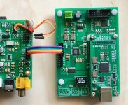
A picture of my dac with one of the AK4137 boards connected to the I2S input can be seen below. You would do the same basic thing, then use the AK4137 board to select USB, coaxial or optical. Hard to see but the optical input connector is under the XMOS board. Actually, the terminals marked RCA and BNC are both coaxial SPDIF inputs, so you get two of those.
Modding the DIYinhk dac to add coaxial SPDIF should be trivial if you know any electronics.
Or, if you did the smart thing for better sound quality and put one of the more fancy AK4137 boards between the XU208 and the DIYinhk I2S input, it has both SPDIF and TOSLINK (coaxial and optical) inputs too (you even get AES), so it would take care of everything for you: AK4137 DAC SRC Audio 384K 32Bit DSD256 DSD IIS Conversion board for hifi power amplifier-in Amplifier from Consumer Electronics on Aliexpress.com | Alibaba Group
A picture of my dac with one of the AK4137 boards connected to the I2S input can be seen below. You would do the same basic thing, then use the AK4137 board to select USB, coaxial or optical. Hard to see but the optical input connector is under the XMOS board. Actually, the terminals marked RCA and BNC are both coaxial SPDIF inputs, so you get two of those.
Attachments
Last edited:
Hello Blackfear,
The bits of that new board important for sound quality are essentially the same as the earlier boards.
The new version you linked to has some very minor changes the dac functionality, mainly much of the circuitry has simply been rotated 90 degrees to make room for a bunch of status display LEDs and a bigger microcontroller to run the LEDs. All the changes are worthless in terms of sound quality, IMHO. Also, this new version looks like it might be worse in terms of ease of modding due to the tighter spacing of some of the dac components.
Hello, that is what I thought...still the same I/V circuit and also remains seems to be the same +/-.
Regarding my discrete HDAM circuit, one man told me regarding better stability:
put resistance directly at the entrance before input EES P, he told me that input of HDAM is fully feeded by current and so it must be voltage-symmetric, so there could be up max. to 1k6. The feedback must be the same resistance as in the positive input, that is the gain symmetry.
I do not quite understand this well..why shall i put another resistance before..i have there the same resistance now... .can you look on it... but what only helped me with stability yet was decreasing C5 in feedback ten times smaller so from 2.2nF to now 220pf...(i saw this on similar differential circuit filters..)
Thanks, Vita
Attachments

Hello again Mark, as you can see i found "similar" discrete schema where we can see some capacitors and resistances values, feedback capacitor is also here 10x times smaller as on mine circuit, but there is also 1k feedback rezistor-LF2 to ground so why there is such rezistor ? also we can see input rezistor Lri 2k2, can you look on it ? thanks 😛
Attachments
HDAM circuits that I have seen used to be in old Marantz CD players and were kind of like single input unbalanced voltage amplifiers. If bringing out two inputs, it would sort of be like a discrete opamp. That is, ideally you would need 3 HDAM circuits for each Q2M dac channel, or 6 HDAM circuits in total. Then you would use 2 for each channel as I/V converters, and 1 as a differential summing amplifier.
However, it appears you don't want to make a lot of HDAM circuits so you are trying to use two HDAM circuits to replace the dual opamp that comes with the unmodified dac board.
That would probably not be a great idea, and could not particularly be expected to make better sound quality than trying a bunch of different opamps in the socket of an unmodified dac board. The main difference is that you don't know the gain and phase characteristics of your HDAM semi-opamp circuits. In other words, you do not know if they approximate very good opamps. You have to know that stuff to calculate what kind of feedback would be needed for stability. Normally you would study basic feedback circuits probably in the 3rd year of a 4-year EE degree, and maybe come back to study them later in more detail in other later courses.
Anyway, as it is now you would be loading the dac output with an intermediate impedance somewhere between voltage mode and current mode. With ESS Sabre dacs there is no advantage to doing that. We already know they work best in current mode offset to AVCC/2.
Well, if you are convinced you want to use this circuit and you don't know how to break the feedback loop and measure loop gain and phase, then calculate approximate feedback values and test, and then possibly empirically fine tune final feedback values for good stability and to meet design goals -- then however you have to mess with it to make it stable and not oscillate is probably about all you can do. However it sounds is how it will sound.
Also, it should be okay to have C5 and C6 small if that makes it stable. Those two caps should be probably be matched so whatever you use for C5, just make C6 the same and see how it sounds. Also, R14 could be connected at the input of R13 like C5 is. That would probably make more sense in this case, it seems to me anyway.
Last edited:
Wanted to show what would be involved in soldering an LT6655 precision, ultra low noise voltage reference to an adapter board for use as an AVCC reference. I would definitely recommend practicing with some SMD parts first just because LT6655 aren't cheap, maybe $7. Good news is it would only take one which could be shared by both AVCC channel opamps (one dual opamp).
Good write-up, thanks!
When populating bare PCBs with SMD components, I've had good luck with the frying pan + stovetop "reflow" method. I use a toothpick to paint solder paste on the PCB pads. Then I place all the components with tweezers. I let the skillet heat up on medium heat, put the PCB on, then crank the heat up to max. I watch as the solder paste turns molten (might have to push the board around a bit), wait a couple seconds, then remove the board and let it cool. The fun part is watching the paste turn molten, which usually straightens and centers any components that weren't placed perfectly. In this post, I elaborated on these steps a bit along with some pictures.
I've read about people doing the same thing in a more precise manner with their cooking oven. I'm not comfortable with the off-gassing in the actual oven we use to cook food. But some day I want to see if I can get a cheap toaster-oven from a thrift store to dedicate to this purpose.
Past the edit window, but I should also add: I originally did SMD work by hand with a soldering iron. But I started the skillet reflow method because I had to solder a device with a ground pad that was "face down"; in other words, the pad served as a thermal bridge between the IC and a (presumably large) copper pour on the PCB to act as a heatsink. Since the chip housing completely surrounds the exposed pad, and mates fully to the PCB, there's no easy way (that I can determine) to solder this with an iron.
(FYI, this was the TPA3118 amplifier chip, but I think this is not uncommon, e.g. the LT3045 has this too.)
I think a lot of people will use a heat gun in this case. And indeed the YouTube videos I watched on the poor-man's reflow technique described above were actually done with a heat gun, rather than stovetop skillet.
Just trying to give everyone more ideas for ways to tackle SMD soldering! I used to be scared of it too. But I can comfortably do 603-sized components and up with my naked eye. And if doing a lot of components on a bare board, using the technique described above, I find it's actually faster than through-hole.
- Home
- Source & Line
- Digital Line Level
- ES9038Q2M Board