Is this correct PM GM measurement procedure?
About Zobel at the output, someone wrote here the amp should be stable in the sim without Zobel. I have it on PCB, btw.
If a 1uF capacitor is used for testing with the speaker, the proper cable itself can have 0.22R series resistance
For the purposes of the simulation make the 0.22R a resistor and not part of the speaker lead.
To make your simulation work copy the following expression and use the .op command to paste it somewhere on your .asc file as a comment
-1/(1-1/(2*(I(Vi)@1*V(x)@2-V(x)@1*I(Vi)@2)+V(x)@1+I(Vi)@2))
From this convenient access point you will be able to paste this in the title field of the .raw file when you run this. The title field at the top of the .raw field will be in green and read V(vout). Click on this and a dialogue box will appear - delete this and substitute the expression given above.
From there the same procedures you applied to set the cursors.
Isn't the main goal here is to choose lowest possible value to decrease distortion?You could try 100pF as your next step.
I'm powering the amp with 100-150W light bulb. I think now it's safe enough to try direct mains connection.
Isn't the main goal here is to choose lowest possible value to decrease distortion? I'm powering the amp with 100-150W light bulb. I think now it's safe enough to try direct mains connection.
There is what is known as a diffusion capacitance between the collector of a transistor and its' base. The value of the capacitance depends on the voltage applied at the collector and has an inverse relationship to the square root of such applied voltage.
If a load is included in the collector circuit - which is the case in a Vas then the voltage at the collector will alter with signal input level and you will have a capacitor of variable value.
You can clean up the defective capacitance by swamping this with a large enough capacitor added in parallel.
You could see this as like a mopping up exercise to clean a muddy floor - no-one thinks of diluting the cleaning agent if they want a squeaky clean result.
Re connection to the mains you should take the precaution of fitting 100R 5 watt resistors in the power stage supply rails and ensure firstly that these do not get hot and secondly the the voltage drop across these can be changed by the Iq adjustment to between close to 0 and say 10 volts.
Do this with no signal input and no load connected. If you get a satisfactory result reduce the Iq to the lowest possible setting and remove the 100R resistors and connect the supply rails directly.
You can then adjust the Iq setting in small increments while monitoring the heat and the voltage drop across one of the power transistor emitter resistors. Allow some time between adjustments for the amplifier to settle - you could spread the process out over half an hour. When you get to the final value for Iq keep monitoring until you feel the amplifier is properly settled.
Also ensure the dc offset remains at a safe level.
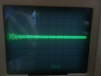
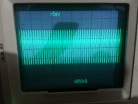
I changed predrivers' base compensation to 165pF and removed R36, R39 10 Ohm VAS collector series resistors (replaced with jumpers). With these caps the amp starts with scope's 10mV (2 rows at 5mV deflection) oscillation and -110mV offset, which (osc and offset) fades out almost completely in 5-10 min, when offset stabilizes close to zero. However when offset changes at least to -45mV due to forced aiflow on the IPS\VAS, osc. appears again and eventualy disappears after a couple of minutes even at -50mV offset. From this observation I can come to a conclusion that osc is highly dependable on thermal (or beta) disbalance of IPS or VAS tr-rs. Btw, my VAS and predriver TO-126 tr-rs aren't matched as small input ones, they have 160 vs 210hfe between npn and pnp.
What do you mean by this? I'm not using 100R 5W and I don't have such resistors to try.
Seems like 44p VAS compensation is enough. Perhaps I should try lower 30p value.
Re connection to the mains you should take the precaution of fitting 100R 5 watt resistors
What do you mean by this? I'm not using 100R 5W and I don't have such resistors to try.
Seems like 44p VAS compensation is enough. Perhaps I should try lower 30p value.
Attachments

Last edited:
It is not a big expense to buy these. You should have fuses in your dc supply rails in case the output stage is ever short circuited. If you don't have any holders that is a trip to the shop.What do you mean by this? I'm not using 100R 5W and I don't have such resistors to try.
You can solder the 5W resistors ( wire wound) across the ends so these will be in series with the supply for test purposes in a way that they don't get in the way when it comes to fitting the fuses when the amplifier is running properly.
I have explained this test method more than once in this thread.
I have to go to another city to the electronic shop. I would better buy 20W types.
There are 15A SMD fuses on PCB just after terminal connectors.
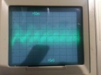
Is it safe to use the amp with such oscillation as I described and showed?
There are 15A SMD fuses on PCB just after terminal connectors.
Is it safe to use the amp with such oscillation as I described and showed?
Attachments
Last edited:
You are still strugling with this ?I changed predrivers' base compensation to 165pF and removed R36, R39 10 Ohm VAS collector series resistors (replaced with jumpers). <snip>
And stable without load or signal.... ??
Have a nice "trial and error" weekend (???) unless you folow somthing already suggested.
Not exactly strugling, but have a lack of understanding of current behaviour of the amp. Roughly I can say there is no osc, as it disappears in time, that means compensation works. I put back again 200p base comp btw. From other side, why osc appears at power on and with DC offset or tr-rs temperature (beta) change? Perhaps there is some tr-rs partial damage from overheat or overload. I don't have curve tracer to check.
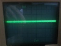
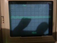
With 4-8R load and without input signal.
Btw, I rebuilt the second channel exactly the same as this first one (with vbe multiplier bias current) and it's totaly stable at power on on the scope with stable DC offset.
I followed already sugested and chose the best out of it.
Anyway, taking into account perfectly stable second channel in my current conditions, we may consider the problem is solved.
Last edited:
To make your simulation work copy the following expression and use the .op command to paste it somewhere on your .asc file as a comment
-1/(1-1/(2*(I(Vi)@1*V(x)@2-V(x)@1*I(Vi)@2)+V(x)@1+I(Vi)@2))
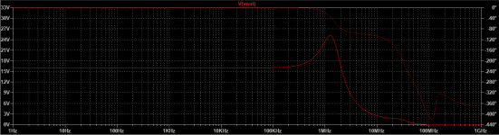
I tried to check the PM\GM with the RDijk file from post 786 and found 62 degree of PM and 15.7db of GM (where the lower limits are 60degree\12db) wih 100p base and 8p VAS compensation. Have I done it right? Does it difficult to check pm\gm in real circuit?
Attachments

Last edited:
I tried to check the PM\GM with the RDijk file from post 786 and found 62 degree of PM and 15.7db of GM (where the lower limits are 60degree\12db) wih 100p base and 8p VAS compensation. Have I done it right? Does it difficult to check pm\gm in real circuit?
You have executed the graph correctly. There will be elements of stray capacitance in the layout that you cannot account for in a simulation.
The best you can do with an oscillator and an oscilloscope is to run a square wave test with a dummy load and see how well this is reproduced. Do this with a 50kHz in the first instance.
Depending on the result the next step would be to include a small capacitor in parallel with the dummy load. I suggest doing this at low output with an external series resistor of say 1R into 8R//47nF.
For this and the remaining tests reduce the square wave frequency setting to 10kHz.
You can read from the time base from zero to the top of the wave form where the level is flat to work out the settling time - the latter is a parameter mentioned in the data for fast varieties of IC op.amp.
With caution you can increase the signal level and reduce the buffer resistor value depending on the settling time which should be less than 10uS and the accuracy of the shape of the waveform. In my view this circuit will need either a buffer resistor of 0.22R or failing that an output coil.
If these tests are negotiated successfully you can repeat the process progressively using your discretion with higher value parallel capacitors.
Be very gentle with increasing signal levels for the higher value capacitors.
If you run into problems you should refer back to the simulation and change capacitor values to increase the stability margins.
Do you mean external series resistor 1R at output or input? And 8R dummy load with 47nF in parallel?
Perhaps better would be to perform these tests with new optimized pcb? Do you think the schematic is complete for new layout? The doubts left only in compensation values.
Perhaps better would be to perform these tests with new optimized pcb? Do you think the schematic is complete for new layout? The doubts left only in compensation values.
External series resistor at the output and 8R in parallel with 47nF. You should try first a 50kHz square wave into the 8R dummy load alone with the amplifier as it stands with a range of low level input signals.
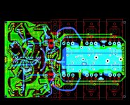
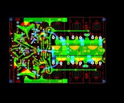
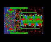
I've made a layout for this sim file. I added 10R GND resistor as per original schematic. There are two gnd planes, at IPS section and as output zone. One thing I'm not sure with gnd planes, as this is not visible in the layout, is how opposite layer components go through these gnd planes.
Comments and offers are welcomed.
Comments and offers are welcomed.
Attachments
Last edited:
I may believe that it can be true, but using gnd plane turns out with much compact and easier layout than if I route gnd tracks separately. It's beneficial in two points: simplicity and noise immunity.
In fact Douglas agreed as well gnd plane can be beneficial in post 115, as I understood.
Sorry, previous image was without GND plane, I thought I uploaded the correct one. Chris, please replace the image with this one. Thanks.
In fact Douglas agreed as well gnd plane can be beneficial in post 115, as I understood.
Sorry, previous image was without GND plane, I thought I uploaded the correct one. Chris, please replace the image with this one. Thanks.
Attachments
Last edited:
if you still have motivation, OITPC appears to offer up to a factor of ten lower THD at 20kHz but in practice there are likely issues hidden from us using our inadequate simulations so it may take a lot of effort to succeed with OITPC. But it would be nice if OITPC works well first try!
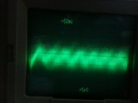
I tried this compensation but I left C13 as 320uF, forgot to replace it. The results are worse than with previous compensation. The amplifier is a bit unstable, I can only bias the input only to 3mA, likewise too much noise from the speaker. Here are the scope screenshots without input signal (first start up and couple of minutes run) and two with input signal.
Attachments
Ian, have you checked that compensation for overshoot?
The phase margin is increased by the means of a resonance after the unity gain frequency. Are you sure the Q of this resonance will remain stable under dynamic conditions considering the Ft of the output transistors may vary 5x or more?
Furthermore this compensation provides a path for frontend rail noise to be injected directly into the VAS input. The simulation does not include modulation of the frontend rails. To fix this the compensation would need to be split into two sections, one for the positive VAS and one for the negative VAS. R44 will be split into two resistors going to their respective rails rather than to ground.
The VAS uses the rail as it's reference node, therefore referencing the OITPC to ground through R44 causes a reference conflict.
Attachments
- Home
- Amplifiers
- Solid State
- One of the Top Solid-State CFA amp design