Since Eoff in IGBT (for no c-e capacitor case and no gate negative bias tricks) does not improve below a certain Rg value, this Rg value resulting in higher td-off is traditionally used for datasheet testing, because td-off helps with desaturation, it improves the abruptness of Ic fall, more in older IGBT, very little in newer. Zero Rg would result in <100ns td-off for the part discussed. On the other hand this small delay is not much of a problem for clocked modulator, and only a slight inconvenience for self-oscillating. I have done good full-range high voltage class D with up to 320ns propagation delay (250khz idle, 25khz flat BW), although smaller circuits benefit from lower like 150ns (340khz idle, 40khz flat BW, smaller output filter).
Negative gate voltage has 2 possible functions. In older transistors (high feedback capacitance) it helps with dV/dt related parasitic turn-on happening after primary turn off. In newer transistors (or busbar style industrial circuits with higher inductance) it can help to increase off di/dt by counteracting the effect of voltage drop across source/emitter lead inductance. Negative gate bias can be achieved statically with a dedicated supply rail, or dynamically with inductors in gate drive and some limiting factors to observe.
Negative gate voltage has 2 possible functions. In older transistors (high feedback capacitance) it helps with dV/dt related parasitic turn-on happening after primary turn off. In newer transistors (or busbar style industrial circuits with higher inductance) it can help to increase off di/dt by counteracting the effect of voltage drop across source/emitter lead inductance. Negative gate bias can be achieved statically with a dedicated supply rail, or dynamically with inductors in gate drive and some limiting factors to observe.
@Eva:
The modulator of Ionut allows clocked and self oscilating operation.
I am not sure in which mode he killed the amp.
In any case I am glad to see that you also promote reduction of fs at high modulation in case of self oscilating designs to be an advantage. Most people see only the negative effects of this.
Regarding switching losses it does not make sense to compare the values at 70A.
At 70A the switching losses at 250kHz plus conductive losses will shoot the junction temperature within some ms from 25C to Tjmax.
Also we do not have to expect 70 Amps with 4R load. More something like 30A..40A.
With respect to typical impedance peaks of speakers reality will be even more forgiving as long as nobody designs a crazy passive cross over.
I know that you know ... Eon must not be ignored in classD applications.
With respect to your five cases: In classD, when running a high power sine wave, each device operates in case 3 for almost 50% of the time. Why did you not mention Eon?
Back to numbers in case 3:
At 35A and 300V the SCT3030AL is specified with Eoff=170uJ and Eon 260uJ, Etotal=430uJ.
At 35A and 300V the IKP30N65F5 will show approx Eoff=260uJ and Eon 750uJ, Etotal will be roughly 1000uJ.
Last but not least. Yes, there is nothing wrong with the Infineon IGBTs, worst case switching losses are just factor 2-3 higher than with SiC. That's definitely very good.
Prices of SiC: I agree. Prices are SiCk. Ingredients and production processes are expensive. Pricing did not turn competitive over the last ten years. Let's see how GaN will evolve over the next decade.
@ Ionut:
Even with SiC the heat concentration in one device is still high,
that's why I proposed to parallel two devices some postings earlier.
Not sure what you want to do: For your living room and some party I trust a single
pair will do the job. For really sick professional cinema applications - not sure.
For continuous sinewaves at 4R close to clipping in clocked mode and below carrier aliasing might happen a single pair will heat up too much after moderate time under any normal heat sinking condition. There is always a way demand more than necessary...
@Workhorse:
I am not so sure if SiC Fets really have a bright future.
IMHO the next 5 years will show if GaN Fets turn more affordable and their formerly issue with dynamic Rdson really is solved, if yes - they have good chances to wipe out SiC Fets.
...or some other fancy wide band gap stuff suddenly turns hip for switches...
Just noticed that I did not mention: If you want to drive such fat SiC Fets with the IRS2092S you will need at least an additional PNP at each Fet for fast turning off. Otherwise your circuit will show Eoff which has nothing in common with the data sheet.
If you intend to parallel two large SiC Fets, then you will need a NPN to boost turn on and a serious PNP for turning off. Of course you can also use a fast gate driver chip.
If you intend to parallel two large SiC Fets, then you will need a NPN to boost turn on and a serious PNP for turning off. Of course you can also use a fast gate driver chip.
Choco,
In my prototype with with SIC, I have experienced the bipolar gate drive +18/-4V with +/-180V rails running at 350khz has less switching losses than unipolar +18V gate drive, whereas my GAN prototype is happy at 7V unipolar drive but requires very fat turn off driver since the Vth is very low. I have even tried PT IGBTs IXGHxxxxC3 series from IXYS as well @ 260khz, the only down side is that you cannot parallel them for high current operation at high temperatures as their VCE_ON decreases with an increase in temperature. GAN is still expensive than SIC presently, I have seen SIC's advantage in inverters for windmills operating at 800V bus at 150khz at elevated temperatures.
In my prototype with with SIC, I have experienced the bipolar gate drive +18/-4V with +/-180V rails running at 350khz has less switching losses than unipolar +18V gate drive, whereas my GAN prototype is happy at 7V unipolar drive but requires very fat turn off driver since the Vth is very low. I have even tried PT IGBTs IXGHxxxxC3 series from IXYS as well @ 260khz, the only down side is that you cannot parallel them for high current operation at high temperatures as their VCE_ON decreases with an increase in temperature. GAN is still expensive than SIC presently, I have seen SIC's advantage in inverters for windmills operating at 800V bus at 150khz at elevated temperatures.
Last edited:
Hi Workhorse,
your findings do not contradict with mine, but you cannot derive a
general rule from it how to drive GaN or SiC.
The requirements for driving GaN and SiC are showing a huge spread. It depends very much on the product family. I would not dare to extrapolate findings from few GaN or SiC devices to GaN or SiC in general.
GaN devices can range from pretty cumbersome drive requirements to full compatibilty with standard MosFet gate drivers .
Cree is specifying for the C3M0065090 that a negative Vgs shall be used, while Rohm specifies for SCT3030AL in the recommended operation no need for negative Vgs.
Like always in power electronics the only way to see why/where/when the losses are happening is to measure the switching events with the particular device.
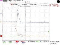
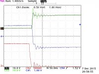
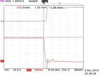
Attached three measurements with C3M0065090. All showing the turn off of the low side switch when the halfbridge is sinking current. All without driving negative Vgs.
The first one is directly driven from the IRS2092 (10R and diode), here the fall time of the current is about 50ns.
The second one is with an additional PNP for the gate, now the fall time of the current takes about 15ns which is already touching the best case from the data sheet and was easily fine in order to mod LiteAmp to the same power level like my 2kW design.
Also note the unpleasant oscillation caused by the parasitic inductance of the wire loop + current probe, already making me afraid at 25A.... The last picture shows the situation without current probe at a current level of 40A.
Picture 1: Directly driven from IRS2092 with 10R and diode. Ch3 not used
Picture 2: With PNP.
Picture 3: With PNP. No current measurement. Ch3 and Ch4 not used.
Ch1: Vds directly at the device pins, 100V/Div.
Ch2: Vgs, 5V/Div.
Ch3: Vds including voltage drop of wire with current probe, 50V/Div.
Ch4: Ids, 10A/Div.
your findings do not contradict with mine, but you cannot derive a
general rule from it how to drive GaN or SiC.
The requirements for driving GaN and SiC are showing a huge spread. It depends very much on the product family. I would not dare to extrapolate findings from few GaN or SiC devices to GaN or SiC in general.
GaN devices can range from pretty cumbersome drive requirements to full compatibilty with standard MosFet gate drivers .
Cree is specifying for the C3M0065090 that a negative Vgs shall be used, while Rohm specifies for SCT3030AL in the recommended operation no need for negative Vgs.
Like always in power electronics the only way to see why/where/when the losses are happening is to measure the switching events with the particular device.
Attached three measurements with C3M0065090. All showing the turn off of the low side switch when the halfbridge is sinking current. All without driving negative Vgs.
The first one is directly driven from the IRS2092 (10R and diode), here the fall time of the current is about 50ns.
The second one is with an additional PNP for the gate, now the fall time of the current takes about 15ns which is already touching the best case from the data sheet and was easily fine in order to mod LiteAmp to the same power level like my 2kW design.
Also note the unpleasant oscillation caused by the parasitic inductance of the wire loop + current probe, already making me afraid at 25A.... The last picture shows the situation without current probe at a current level of 40A.
Picture 1: Directly driven from IRS2092 with 10R and diode. Ch3 not used
Picture 2: With PNP.
Picture 3: With PNP. No current measurement. Ch3 and Ch4 not used.
Ch1: Vds directly at the device pins, 100V/Div.
Ch2: Vgs, 5V/Div.
Ch3: Vds including voltage drop of wire with current probe, 50V/Div.
Ch4: Ids, 10A/Div.
Attachments
Ch1: Vds directly at the device pins, 100V/Div.
Ch2: Vgs, 5V/Div.
Ch3: Vds including voltage drop of wire with current probe, 50V/Div.
Ch4: Ids, 10A/Div.
Correction of some typos:
Ch1: Vds directly at the device pins, 100V/Div.
Ch2: Vgs, 5V/Div.
Ch3: Vds including voltage drop of wire with current probe, 100V/Div.
Ch4: Id, 10A/Div.
...had a closer look to the data sheet of the driver.
It has a nice strong output: In terms of current capability it might
work to drive the SiC Fets directly with 6R8 for turn on and shottky+2R2 for turn off - but I guess thermal stress will be to high (did not calculate..).
Simply step into the equations of the data sheet and you will see if the driver will run hot or not. Be prepared to use two external PNP in order to shift heat from the driver to the external components.
P.S.
Have a closer look to your layout and minimize parasitic inductances, otherwise you will not be able to take full advantage of the Rolls Royce devices you have on your desk.
Hi Workhorse,
your findings do not contradict with mine, but you cannot derive a
general rule from it how to drive GaN or SiC.
The requirements for driving GaN and SiC are showing a huge spread. It depends very much on the product family. I would not dare to extrapolate findings from few GaN or SiC devices to GaN or SiC in general.
GaN devices can range from pretty cumbersome drive requirements to full compatibilty with standard MosFet gate drivers .
Choco,
I am not generalizing, My observations are based on SIC from Cree and GAN from Transphorm as samples. What I have found is that negative drive definitely helps in the case of SIC.[Yet to check the same with ROHM, awaiting samples, will let you know if the parameter spread is same or different and if negative turn off helps or not], Unfortunately with GAN the turn-off has to be extra strong to keep them sleeping when not active else lot of fireworks and they are very layout crazy.
In my industrial inverter adventures, I haven't seen a single SIC being driven unipolar, always bipolar drive +18/-4V
Last edited:
Cree is specifying for the C3M0065090 that a negative Vgs shall be used, while Rohm specifies for SCT3030AL in the recommended operation no need for negative Vgs.
Like always in power electronics the only way to see why/where/when the losses are happening is to measure the switching events with the particular device.
Attached three measurements with C3M0065090. All showing the turn off of the low side switch when the halfbridge is sinking current. All without driving negative Vgs.
In your case the max absolute rail voltage is limited to less than 200V[+/-100V][IR gate drivers IRS2092/20957] and current is no more than 50A, unipolar drive might do. In my case the rails dance from +/-190 to +/-230VDC with current touching 100A very easily , I did tried unipolar gate drive, had instances of field failures during high current high temperature operation. Then switched to bipolar gate drive for ultimate reliability, never came across any failure anymore. There is nothing to contradict, the application environment is different in my case.
Yet to check the same with ROHM, awaiting samples, will let you know if the parameter spread is same or different and if negative turn off helps or not
..thanks, I am definitely curious. Correlating experiences with theory and data sheets is helpful to improve predictions.
As mentioned in my posting #38 for the Cree devices C3M0065090 the data sheet let's expect issues in reliability without neg. Vgs, even when it works on my desk under nice lab conditions.
Which Cree devices are you using?
The Rohm data sheet SCT3030AL looks like it should be Ok with unipolar drive. In fact SCT3030AL looks even critical regarding bipolar drive, because Vgs must not go below -4V.
Which Rohm device are you going to examine?
I have used C2M0040120D from Cree in my prototype which is still operational in field for extended testing.
Even ROHM in their app note for SIC section 3.9, P15 recommends negative gate drive.
If high noise tolerance and fast switching are required, negative
voltage of approximately -3 to -5V can also be used
I am after SCT3017AL, would love to see what happens at 100C operation.
C2M0040120D: Thanks for sharing your experiences and also good to see that the recommendation in the data sheet is fitting.
SCT3017AL: Looking forward to your findings. Data sheet let's expect that
no negative Vgs is needed (alike for the SCT3030AL).
In case you find that you would need negative Vgs:
How are you going to handle the absolute max rating of Vgs which must not go below -4V? Fast clamping directly at the pins?
Or would you judge it in this case as an unusable component, because of insufficient margin between absolute maximum ratings and real life drive needs?
To add further,
Normal Mosfet with series Schottky and anti parallel Fred combination is still the winner as far as cost is concerned, though a bit more on pcb space and marginally less efficient.
Are you sure?
You have to pay for three power components plus isolation materials and mechanical works.
To me the IGBT approach appears attractive in terms of money. Even when you do not buy it directly in large volumes at Infineon, but buy it at a distributor... price for 1k looks promising:
IKP30N65F5 Infineon Technologies | Mouser Deutschland
In case you find that you would need negative Vgs:
How are you going to handle the absolute max rating of Vgs which must not go below -4V? Fast clamping directly at the pins?
Or would you judge it in this case as an unusable component, because of insufficient margin between absolute maximum ratings and real life drive needs?
Till date all my gate drivers have dedicated floating gate driver supplies, I don't like bootstrapping. In case of negative drive, I have already done it with regulated levels which keeps it within +18/-4V. Hence no problem with Cree SIC which has absolute max VGS rating of +25/-10V.
In case of ROHM device I am little skeptical about its VGS rating mentioned in its datasheet. The margin should be there or there is no need of negative drive at all. But the appnote says -4 to -5 V which means tolerance is higher. Need to confirm it for sure.
Last edited:
Yes, because the cost of the MOSFET + Schottky + Fred is still lower than the SIC of same rating.Are you sure?
You have to pay for three power components plus isolation materials and mechanical works.
To me the IGBT approach appears attractive in terms of money. Even when you do not buy it directly in large volumes at Infineon, but buy it at a distributor... price for 1k looks promising:
IKP30N65F5 Infineon Technologies | Mouser Deutschland
I have not tried Trench stop IGBT so far, hence can't comment but it looks like it's right time to do it, who knows we get something interesting. I believe that these have positive tempo , hence their VCE ON increases with temperature and thus these could be paralleled.
To add further,
Normal Mosfet with series Schottky and anti parallel Fred combination is still the winner as far as cost is concerned, though a bit more on pcb space and marginally less efficient.
Also a matter of the voltage levels of the DC-Link. SiC devices have the singular advantage of 1200V (and even higher) breakdown voltage. Of course, this is not really a topic in class-d.
Here are some results with ipp410n30, +/- 145v, 3.8 ohms load, 50hz sinusoidal input. As only a portion of the sinusoid is displayed, the Vpp value must be composed of Vtop x 2, resulting in 250v pk. You can also appreciate the time when I asked for this power. I also connected a speaker with a resistive divider, so that sound can be heard at that power (unfortunately, there is a lot of ambient noise). Whoever tried it knows what to look in this case. Who has not tried yet, should do it.
YouTube
YouTube
...had a closer look to the data sheet of the driver.
It has a nice strong output: In terms of current capability it might
work to drive the SiC Fets directly with 6R8 for turn on and shottky+2R2 for turn off - but I guess thermal stress will be to high (did not calculate..)
For this gate drive configuration, Fsw=250khz and Vcc=18v results Pd=530mw and 55 degree temperature rise.

- Home
- Amplifiers
- Class D
- Class D amp with 300v mosfets