Hi folks,
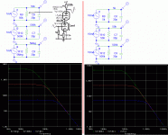
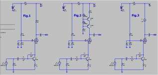
I designed a hybrid cascode stage in LTspice (Fig.1) that offers good performance, with a frequency response well extended.
Then I wanted to replace load resistance with an active load (BJT), so I modified the scheme as in Fig.2.
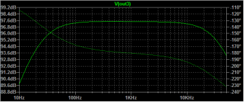
The triode working condition (Va, Ia, Vg) is practically the same as the previous schema, but the gain has increased tremendously and the frequency response is very limited.
I replaced the active BJT load with a CCS (Fig.3), getting the same result.
Can anyone help me understand the reason such a bad freq. response?
Thanks.
Albert.
I designed a hybrid cascode stage in LTspice (Fig.1) that offers good performance, with a frequency response well extended.
Then I wanted to replace load resistance with an active load (BJT), so I modified the scheme as in Fig.2.
The triode working condition (Va, Ia, Vg) is practically the same as the previous schema, but the gain has increased tremendously and the frequency response is very limited.
I replaced the active BJT load with a CCS (Fig.3), getting the same result.
Can anyone help me understand the reason such a bad freq. response?
Thanks.
Albert.
Attachments
Gain-Bandwidth product.
The DC (low audio) gain may be manipulated quite high.
NO amplifier has gain to infinity, so must always have a falling high-frequency response.
For simple amplifiers, this gives two lines on the frequency plot. Straight from DC to a point where it intersects the inherent high frequency slope line.
By cascoding you can increase the resistance but do nothing for the capacitance.
> I must to forget
I did not open the .ASC file. I do not have that program. It might be good to post the circuit and response graphs so more people will comment.
I did not open the .ASC file. I do not have that program. It might be good to post the circuit and response graphs so more people will comment.
I can't read your ASC file. But a cascode is basically an AC current source. So to show the concept I used SPICE's AC current source. We often run audio tubes near 1mA, so I set peak current to 1mA.
The simplest audio cascode uses a resistor load. The size is limited by how much DC drop we can afford. It is usually not-large compared to cascode output resistance. I assumed two units of 6DJ8 at around 2.4K*33*33 or 80K internal impedance, 133K DC resistor, 50K total resistance, in parallel with whatever load it drives (do not neglect this).
But with an "active load" we can have small DC drop and large AC resistance. Gain will increase. I plotted 500K and 5meg. (The 5Meg case works in voltage regulators to reject mains frequencies below 1KHz.) Note that 1mA in a 5meg resistor is 5,000 Volts; this "has" to be an active load.
There is *also* ALWAYS capacitance. Unless layout is very tight and next-stage is buffered, 30pFd to 100pFd would be typical.
The low frequency gain goes up with resistance. The high frequency gain is dominated by the 30pFd, and the same for all resistances.
What you need to drive capacitance at high frequency is big current. If you have an active load, you may be able to pass big current and get high AC impedance without large DC voltages. I pushed the AC current source up 10X, made all resistors 10X smaller. You see the low frequency voltage gains stay the same, but the high frequency corner is 10X higher.
In transistors you can indeed run 10X more current. In tubes, transconductance does not go up as fast as current, so you may need 50X to 100X more current, which is usually absurd. But 2X-3X more current is often worthwhile.
Attachments
Last edited:
I digged a little deeper, but the core reason still seems to remain out of reach.Can anyone help me understand the reason such a bad freq. response?
The primary reason for the frequency distortions is the huge increase in gain seen by the lower driving transistor: something like 40dB.
This means that due to local feedback, the 47µ coupling capacitor becomes significant, as is the Miller capacitance of the transistor.
This is a purely mechanistic explanation, and it doesn't address the main issue: why is there such a gain increase?
Again, an automatic explanation is that the impedance seen at the cathode has undergone a huge increase, but frankly, I don't see why an increase of the anode impedance, even to near-infinity, could have such an effect.
Maybe it could, I should write the equations down, and the answer might magically appear, but my gut feeling is that the impedance seen at the cathode will always be close to 1/gm, whatever the anode load is (but I am basically a semiconductor guy, and some aspects of vacuum could well escape me, unless I do things in a proper, mathematical way)
> I must to forget
I did not open the .ASC file. I do not have that program. It might be good to post the circuit and response graphs so more people will comment.
I have upload the schemes and their frequency response.
I hope this help you to give me some practical suggestion. I'm sorry but because of my poor English, I'm not sure to fully understand all your reasoning ...
Thanks.
Attachments
my gut feeling is that the impedance seen at the cathode will always be close to 1/gm,
whatever the anode load is
That's right, the lower device has little voltage gain (due to that low impedance loading it),
so its own gm converts the input voltage into current that flows through the next stage's load,
avoiding the CCS. That CCS itself may the the bandwidth bottleneck due to its shunt capacitance.
Last edited:
Could the the value of R12 at be a little to high
to provide enough bias for Q1 at higher frequencies?
to provide enough bias for Q1 at higher frequencies?
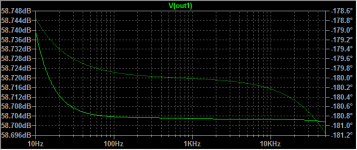
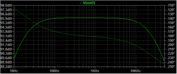
the gain has increased tremendously and the frequency response is very limited.
The load impedance:
1.) 25k;
2.) few 100k..1M (BJT CCS);
3.) infinite (ideal current source).
The gain increasing is natural.
The freq. response of last two is appropriate, aside from the unreal gain.
Attachments
What an odd way to build a cascode. High apparent voltage gain, but very low input resistance. Assuming BJT gain of 100, and Re of 25, the input impedance will be near 2,500. Adding hie and seeing this BJT has gain like 900, maybe 30K. In shunt with the 267K and its Miller effect.
The resistor-loaded cascode: gain is 860 or 58.7dB all the way to 50KHz. By inspaction of Rx=25r and R20=25K we know gain is 1,000 or 60dB at most. Including some small resistances, 58dB is reasonable. The deviation 20Hz-20KHz is 0.01dB. It looks odd that response *rises* below 20Hz, but look at the plate load. It is 25K while C8 is in control, rises to 29.7K when C8's reactance rises.
By my simulation, gain is 10 (20dB) at 87MHz, unity at 270MHz.
58dB is a LOT of gain for any audio purpose. 270MHz unity gain is incredibly high for audio. If you really want all of that, you did very well.
Now use a current source instead of a resistor. The DC gain goes way up, 31,000 or 90dB!! But -3dB at 60KHz, then gain falls off more: 10 (20dB) at 87MHz, unity at 270MHz. Same as before.
Note also that the output impedance rose from 25K to about 900K. If the next stage has a 1Meg grid resistor, gain will be half. If it has *any* capacitance (there is capacitance everywhere) the high frequency gain will be less. You probably can not come close to the calculated performance in any real-world audio system.
By the way: in my simulation, a 6.5mA current source pulls the Plate up to only 8V less than the supply. Very little audio swing. 4mA seems to be a more happy condition.
I = 4mA
Vgrid = 1.25V
Vplate = 126V
Vemitter = 0.1V
Vbase = 0.8V
Vcollector/cathode = 5V
This hybrid cascode stage is thought for input phono MC (first stage).
Second stage will be a dc coupled cathode follower.
I hope this help...
Second stage will be a dc coupled cathode follower.
I hope this help...
I think I understand why the transistor alone acquires such a high gain: the impedances around the triode become so high, much higher than the tube's internal resistance to the point of "shorting" the tube, defeating its cascode role and raising its cathode impedance.
A pathological mode of operation, if you want my opinion.
A pentode would probably behave more normally in these conditions
A pathological mode of operation, if you want my opinion.
A pentode would probably behave more normally in these conditions
Because you have a constant current source in the load, this affected the gain of transistor (60+dbs) cascade to tube (30+dbs), gives a total of 90+dbs. The poor response has to do time RC constant in the input, C6, C3 and C10, changed to 470u straighten the bottom end, while the gain remained the same. The input signal is too high try to reduce it to 1mV from 24mV, but does not effect freq. response however.
> the impedances around the triode become so high
That's a key trick to making DC-LF gain. You can try to take it as far as you want. It does not help high frequencies a whole lot (Miller effect, but that is moot on MC needles).
Let's take two obvious alternates. The original BJT alone has quite large "plate" resistance, and can make high gain if the load is infinite. Modern real BJTs have Mu approaching 10,000. Old SPICE BJT models may only assume Mu>1,000. We expect a gain near 60dB.
BJT plus a 6DJ8 "should" be 33 times or 30dB higher impedance and voltage gain.
BJT plus another BJT cascode "should" be 1,000 times or 60dB higher impedance and voltage gain.
My idiot assistant gives roughly these numbers, see attached.
Note that these plots assume an INFINITE load. The I-source or CCS is never infinite. Neither is any sort of follower you need to drive real loads. In an all-BJT implementation you expect about 1/3rd or -10dB off these plots, assuming your CCS and follower are real devices/pairs similar to your gain device/pair.
Note that the gains are not that far apart at 10MHz. There are little sneak-capacitances and the increasing Mu does tend to isolate them a little, but not like the cascode effect on DC-LF gain.
An interesting side-light is the droop below 30Hz due to the one input capacitor. Miller effect in 267K lowers input impedance. But when the upper device is a BJT, the low hie makes Miller almost vanish. (However this 2-BJT plan has real bias stability troubles; with real devices it will not just-work as-is.)
Attachments

Last edited:
- Status
- Not open for further replies.
- Home
- Amplifiers
- Tubes / Valves
- Cascode preamp stage - active load in LTspice