Hi,
Here is my final circuit. The improvements on the original D. Self Blameless 50W amp (on page 209 of his Audio Power Amplifier Design
Handbook 5th edition) are the following:
- ThermalTrak output transistors [better quiescent current stability]
- separated current source for LTP and VAS [more symmetrical slew rate]
- OITPC (output inclusive two pole compensation - borrowed from dadod's ultra low distortion amp design). [even lower distortion]
- RC filtering on the +supply and a simple voltage rectifier on the -supply [higher PSRR]
- a 100n capacitor across the bases of the output transistors [lower cross conductance at high freqencies]
Thanks to the 2-pole compensation the distortion is quite low. All distortion products are below -110 dB even at 20kHz 50W / 8 Ohm so they must be surely inaudible. I didn't simulate a 4 Ohm load.
In the real world the distortion should be higher. Spice simulation does not account for many effects, e.g. the non-ideal real life capacitors or the input current distortion (because of the LTP nonlinearly drawn input currents). If it input curr. dist. is problem for you, remove the input filter (R39, C14), and use a low impedance source (not a volume pot)! Also there may be problems about common mode distortion as some people pointed out in this thread. I wonder how to simulate common mode distortion?
The circuit is not overly complicated and has a large enough phase margin (I didn't push the compensation so high as could have been done), so perhaps the circuit will not be prone to oscillation even if the layout is not very good. Simulated a 100nH parasitic inductance in the feedback line (can be the inductance of about 10 cm - 4" long trace in a real PCB) and it doesn't upset stability.
I'm not planning to make a PCB for this circuit in the near future. Maybe later...
Still if somebody plans to build it make sure the compensation capacitors (C4, C6, C7) are quality ones, beacuse they are in the feedback paths (no cheap X7R ceramics which distort severly). Perhaps PS or PP foil capacitors are the best here? Or NP0 C0G ceramics? Any advice?
The simulated supply voltage was +/- 37V. In theory can be anything from about 20V to 50V without changing the circuit, only the max. power will be different. As you can see there is no protection circuit so the fuses must provide all there is. Or you can incorporate some protection in your own design.
Here is the zipped asc file + models, in case somebody wants to play around in LTSpice...
Attachments

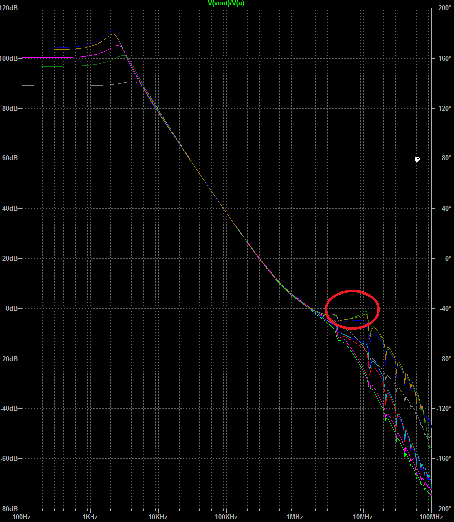
I also don't see C7 doing anything useful while it creates an ugly kink on your loop gain.
Attachments


Last edited:
Bode Step
Classical Feedback Control, Chapter 4: Shaping the Loop Frequency Response
Classical Feedback Control, Chapter 4: Shaping the Loop Frequency Response
Chapter 4
SHAPING THE LOOP FREQUENCY RESPONSE
The problem of optimal loop shaping encompasses two fairly independent parts that can be solved sequentially (thus making the design structural):
The first part is feedback bandwidth maximization which is solved by appropriately shaping the feedback loop response at higher frequencies (in the region of crossover frequency and higher).
The second part is of distribution of the available feedback over the functional feedback band.
The feedback bandwidth is limited by the sensor noise effect at the system output, the sensor noise effect at the actuator input, plant tolerances (including structural modes), and nonminimum phase lag (analog and digital) in the feedback loop. The optimal shape of the loop gain response at higher frequencies, subject to all these limitations except the first, includes a Bode step.
The Bode step is presented in detail as a loop shaping tool for maximizing the feedback bandwidth. The problem of optimal loop shaping is further described and the formulas are presented for calculation of the maximum available feedback over the specified bandwidth.
The above solution is then generalized by application of a Bode integral to reshaping the loop gain response over the functional bandwidth (i.e., for solving the second part of the loop shaping problem). It is shown that the feedback is larger and the disturbance rejection improved in Nyquist-stable systems.
Loop shaping is described for plants with flexible modes, for collocated and non-collocated control, and for the loops where the plant is unstable. The effect of resonance mode coupling on the loop shaping in MIMO systems is considered.
It is described how to shape the responses of parallel feedback channels to avoid nonminimum phase lag while providing good frequency selection between the channels.
It is not exactly applicable here since in 4.2.2 it is described to compensate mostly non-minimal phase lag (and it looks like it is doing it looking at fig.4.2.b). Here, @ ~2MHz it will be negligible. While it may crate a potential problem in interaction with load/cable (as a non terminated TX line etc), considering that with an existing output filter load isolation is not high.
If it is an attempt to compensate variation of ft of output devices (load current, voltage, sample variation etc), it is more safe to do it by manipulation in the feedback divider (adding RC in parallel witр R34 for example), but not adding one more high freq feedback loop around. Interaction with a load sill should be considered.
If it is an attempt to compensate variation of ft of output devices (load current, voltage, sample variation etc), it is more safe to do it by manipulation in the feedback divider (adding RC in parallel witр R34 for example), but not adding one more high freq feedback loop around. Interaction with a load sill should be considered.
Last edited:
In case you'll be referring to Cherrys NDFL designs, as a practical example. He was using pretty heavy degeneration in VAS to ensure stability under different conditions. Also output filter he used would provide a higher isolation from load.
I also don't see C7 doing anything useful while it creates an ugly kink on your loop gain.
That ugly kink is so called Bode step and it is very useful to increase phase margin.
C10 removes small kink in Bode plot, it's explained in Cordell's book.
Damir
I used this type of compensation first time in mine CFA design and as I know it's quite unique never used before.
Attachments
Last edited:
That ugly kink is so called Bode step and it is very useful to increase phase margin.
I know what is bode step. Although, in my opinion, creating it using a local feedback around output devices is a bad idea. As I mentioned before, ft of the output devises varies dramatically with a load current and voltage and power amp load is hardly predictable around those freq in a real life. And it is too close to 0dB line. So yeah, please pardon me, but this is an ugly kink 🙂
C10 removes small kink in Bode plot, it's explained in Cordell's book.
I know what it does, I just don't see a point in doing it. This kink adds gain in your frequencies of interests, it does not remove it.
Vast majority of modern audio DAC/ADCs incorporate DS/PDM modulators with integrator/resonator that deliberately have conjugated poles around this area to maximize gain and squeeze quantization error from the audio band. Why would I remove it by making schematic more complex?
Last edited:
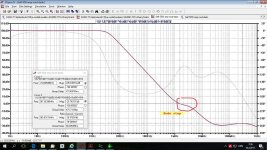
Just to illustrate what I'm talking about. It is quite crude, but gives an idea. Just added stepping trough output voltage (pretty much from top to bottom), a TX line which roughly represents a cable and a few reactive components that represent tweeter winding inductance + parasitic capacitance etc. I've shown where it gets closer to 0dB that it should, in my opinion.
Attachments


I know what is bode step. Although, in my opinion, creating it using a local feedback around output devices is a bad idea. As I mentioned before, ft of the output devises varies dramatically with a load current and voltage and power amp load is hardly predictable around those freq in a real life. And it is too close to 0dB line. So yeah, please pardon me, but this is an ugly kink 🙂?
I don't think that ft varies dramatically for this fast type of output BJT, just between 20 and 40 MHz for working currents and voltages, I don't expect problem here. I built mosfet OPS version with similar compensation with no stability problem at any output power, even at clipping.
I know what it does, I just don't see a point in doing it. This kink adds gain in your frequencies of interests, it does not remove it.
Vast majority of modern audio DAC/ADCs incorporate DS/PDM modulators with integrator/resonator that deliberately have conjugated poles around this area to maximize gain and squeeze quantization error from the audio band. Why would I remove it by making schematic more complex?
It is not strictly necessary but it's just one cheap capacitor.
Without it the loop gain is a bit higher but the phase changes are higher too.
Last edited:
I don't think that ft varies dramatically for this fast type of output BJT, just between 20 and 40 MHz for working currents and voltages, I don't expect problem here. I built mosfet OPS version with similar compensation with no stability problem at any output power, even at clipping.
Well, first of all, it varies a lot. And this is only at two given Vce.
Imagine what is happening when it drives a complex load with a woofer and its filter.

Second of all, the main contributor here is not the ft, but poor isolation from load around this freq region.
And the last, but not least. This amp would be perfectly stable just without this cap or with a small adjustments. Why would you add something that only pushes it toward stability problems?
It is not strictly necessary but it's just one cheap capacitor.
Without it the loop gain is a bit higher but the phase changes are higher too.
Your resulting error signal still will be smaller, thanks to a higher gain, and as a result phase error at the output also will be lower too. And as I mentioned, most of modern DACs/ADCs modulators have similar looking integrator(s) gain. It does not look like it bothers anyone.
If I would do anything around this area, I would try to stabilize its position. As output voltage changes, loop gain changes too, resulting in shifts of those poles (can be seen on plots I've shown).
Last edited:
Well, first of all, it varies a lot. And this is only at two given Vce.
Imagine what is happening when it drives a complex load with a woofer and its filter.
Second of all, the main contributor here is not an ft, but poor isolation from load around this freq region.
And the last, but not least. This amp would be perfectly stable just without this cap or with a small adjustments. Why would you add something that only pushes it toward stability problems?
Your resulting error signal still will be smaller, thanks to a higher gain, and as a result phase error at the output also will be lower. And as I mentioned, most of modern DACs/ADCs modulators have similar looking integrator gain. It does not look like it bothers someone.
If I would do anything around this area, I would try to stabilize its position. As output voltage changes, loop gain changes too, resulting in shifts of those poles (can be seen on plots I've shown).
Without that cap it's hard to get more then 60 degree of PM and 10 dB of GM and with less loop gain at 20 kHz. With this cap simulation shows 75 degree of PM and 26 dB of GM. I don't see it as pushing towards instability but opposite, to more stability.
I suggest you to build this, you could be surprised.
By the way why are you afraid of feedback around OPS, global negative feedback uses it with no problem.
TMC is also around OPS and many amps use it with no problem, me too in my TMC amps.
Last edited:
Without that cap it's hard to get more then 60 degree of PM and 10 dB of GM and with less loop gain at 20 kHz. With this cap simulation shows 75 degree of PM and 26 dB of GM. I don't see it as pushing towards instability but opposite, to more stability.
I suggest you to build this, you could be surprised.
I'm a bit lost here, why exactly do you need more that 60 degrees of a phase margin?
And again, there is not only phase margin exists, there is also a gain margin, and it has to be present at meaningful value. An this gain margin gets critically low with this mod. How this can be more stable with ~1dB of gain margin closer to 8MHz?
I'm a bit lost here, why exactly do you need more that 60 degrees of phase margin?
And again, there is not only phase margin exists, there is also a gain margin has to be present. An this gain margin gets critically low with this mod. How this can be more stable with ~1dB of gain margin closer to 8MHz?
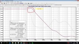
Read it carefully, it's 26 dB of gain margin (GM) with this cap. I presented the Loop Gain plot some post back and you can read PM and GM from it. That was not open loop gain plot but the loop gain plot or feedback ratio plot.
Last edited:
Read it carefully, it's 26 dB of gain margin (GM) with this cap. I presented the Loop Gain plot some post back and you can read PM and GM from it. That was not open loop gain plot but the loop gain plot or feedback ratio plot.
Look carefully here
Or you expect that 8Ohm resistor to represent correctly such a complex load as a speaker connecter trough 3-6m of a cable?
I can vary the line length and speaker parasitics a few times in different direction, and problem still would be there but at slightly different frequency.
Look carefully here
Or you expect that 8Ohm resistor to represent correctly such a complex load as a speaker connecter trough 3-6m of a cable?
I can vary the line length and speaker parasitics a few times in different direction, and problem still would be there but at slightly different frequency.
OK I gave up, this is not mine simulation.
What specifically is wrong with the kink?
I don't think anything is wrong with the kink, Shaq888 is using transmission line to simulate long loudspeaker cable and that was wrong.
It is not exactly applicable here since in 4.2.2 it is described to compensate mostly non-minimal phase...
In 4.2.2 describes how to compensate minimum phase, when Bn(fc) = 0.
This is the baseline case that can be extended to non-minimal phase.
The minimum phase can be an arbitrary amount, while the non-minimum phase is limited to less than one radian.
So I would say it is to compensate mostly minimum phase, with an extension for a limited amount of non-minimum phase.
Therefore it seems exactly applicable here, in my view.
Some of your comments are in accord with my own ideas and the discussion has made me reexamine Damir's compensation.
If you are interested then my comments will be in Damir's thread.
Best wishes
David
- Status
- Not open for further replies.
- Home
- Amplifiers
- Solid State
- Please help improve Self's Blameless 50W amp