No question I am at a disadvantage without test or measurement equipment. Maybe two years ago I borrowed some from an antique radio museum I belong to and am on reasonable terms with one of the directors. That was merely a signal generator and VTOM (which was not sensitive enough) to make record/play level adjustments on a couple of 8 track recorders.
I spent as much time as I could yesterday morning reading from the Elliot Sound Products link. It was certainly not dry reading, the author had a style that kept my interest up. But there is only so much I could read using my old iPhone before my eyes start smarting. I intend on transferring the document via USB drive then take to an office supply store to make a nice crisp (large print maybe even?) hard copy I can read more comfortably. Some think me odd that these days, I prefer reading in this manner. A good friend of mine is a self published author. His sales a primarily downloads and I can obtain those for much less than I must pay for an actual book but I continue doing the latter. I have tried numerous times to do ambitious reading on a screen but for some reason I cannot "absorb" what I've read to the extent I can if I'm holding a book in my hands. Recently that same subject arose on a radio program I listen to. Seems it is documented that in general, readers do comprehend less and retain less when reading on screen.
So I cut to the chase and replaced the 3.9 volt diodes with new ones then measured voltage drop across R435/439 of which there was none. The reading is still 0 volts.
If unnecessary to list individual findings, in general terms, this is what I did next:
I looked for E to C ma current at Q409/411/401/405/402/406. There was none at Q409 and unless I was holding the probes wrong, none at Q405 either. There was ma present at the others but inconsistent (some varied erratically) and were considerably higher than the 1 to 2 ma you say should be there.
Something interesting occurred when doing this at Q411. When contacting probes to E & C the DBT grew noticeably brighter. The meter was reading 150ma when I removed the probes but it was increasing.
I also checked vBE voltage on those transistors. I won't detail the findings as they varied transistor to transistor.
Other than +/- should not the voltage be the same regardless of if the probes are black to B - red to E and vice versa?
Numeric readings were similar in both directions with Q405 and Q402 but not so with the others. Q405 was +/-2.5 volts and Q402 was +/-1.5~1.7 volts.
Last edited:
Additional
Brightening of the DBT when checking mA readings at Q411 E & C made me go back and double check. DBT responded the same way but I also re-checked Q409. I must not have had the probes in good contact with the transistor's legs previously as I now obtained the same result as with Q411 - 150mA and rising plus brightening of the DBT.
To compare, I checked their counterparts Q410/412 which were 0mA and DBT brightness unaffected.
Does this means then that my DMM on mA setting allows current to pass through thereby brightening the DBT? But since the same procedure on Q410/412 had no effect to the DBT, then....no?
I decided there was nothing to loose by replacing Q409/411 and was afterwards encouraged by now obtaining 1.2 volts across R439 instead of zero but there was still 0 volts across R435. Thinking that because they were paired with Q409/411, replacing Q413/415 might be logical but doing so did not produce voltage across across R435 as I expected.
Presently, with the DMM set at mA, touching the probes to C & E of either Q409 or Q411 still causes the DBT to brighten but now only slightly. The current readings still seems to want to rise but start at about 50mA and rises slower. It would take quite a while to reach 150mA and maybe not even get that high.
As a matter of fact the DBT (with 60W bulb) now glows a bit dimmer at idle after turn on than it did before.
Looking to the other channel for comparison, there was no voltage across R440/436, both read 0. I was assuming that side was working but maybe not?
OK, I could not get through yesterday and lost my posts 3 times. I gave up after blowing 4 hours of writing, retyping and waiting, waiting to upload.
I think you may misunderstand the way to measure current with a DMM or current meter. I should have asked or explained the method first before simply saying to 'measure the current'.
First, a current meter must have a low internal resistance so that it doesn't impede the circuit operation in any way. 'Sounds good but what if you were to place that meter across points of high potential difference in circuit? Well, lots of current usually flows and could well take out any components in the current path and any collateral circuits too. I think this is what's happening when you see the DBT glow so please, don't measure this way.
It may seem contradictory and crazy, but generally, don't use the meter's current ranges to measure current - too risky and requires breaking the circuit of interest to insert the probes between the break. Apart from taking time and being a PITA to do, this inserts the meter's own resistance into the circuit and changes its operation to some degree.
If you attempt to measure current in the same way as you measure voltage, you will just be shunting more current between the the 2 test points, according to the internal low value reference resistor in the meter and this is not good at all.
In a DMM set to current ranges, a low value resistor in series with a safety fuse is placed between the probe leads. Current is then read (re-scaled to A, mA etc.) as the voltage across this resistance. If the test points have any appreciable potential difference, that could be quite a lot of current and probably enough to take out any components in the current path. This will certainly light up the DBT if that is what's happening. In a nutshell, don't follow the instructions for measuring current with a DMM and don't try to measure current directly by any other means. Current ranges may be OK for robust circuits but not delicate electronics where it's too easy to make disastrous mistakes.
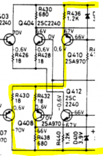
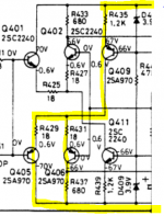
What most here (at least those of us whose gear is still working) do, is use the existing resistors in-circuit to calculate the current, either with a calculator or brain cells and Ohm's law, which becomes an automatic process after a few repairs or builds. Let's use the case of the bias current through one of the input transistor pairs (Q405/406) and their current source or regulating transistor, Q409. R436 is conveniently in series with this circuit and will make a suitable reference, given it will be better than 5% accurate.
Just measure the voltage across the resistor and we should get a ballpark 3V, according to the schematic. Since I= E/R, the current then is 3/1,200 or around 2.5 mA. That 2.5 mA is shared between Q405/406 and you might expect to measure the individual bias currents by then measuring voltage across R429/431 but being only 18R, this will be very difficult, at around 70 uV - a tad small for a DMM. I would not try it, rather just check the Vbe and any C-E short there or just replace them regardless, if I was uncertain and needed to remove them for any reason.
I think you may misunderstand the way to measure current with a DMM or current meter. I should have asked or explained the method first before simply saying to 'measure the current'.
First, a current meter must have a low internal resistance so that it doesn't impede the circuit operation in any way. 'Sounds good but what if you were to place that meter across points of high potential difference in circuit? Well, lots of current usually flows and could well take out any components in the current path and any collateral circuits too. I think this is what's happening when you see the DBT glow so please, don't measure this way.
It may seem contradictory and crazy, but generally, don't use the meter's current ranges to measure current - too risky and requires breaking the circuit of interest to insert the probes between the break. Apart from taking time and being a PITA to do, this inserts the meter's own resistance into the circuit and changes its operation to some degree.
If you attempt to measure current in the same way as you measure voltage, you will just be shunting more current between the the 2 test points, according to the internal low value reference resistor in the meter and this is not good at all.
In a DMM set to current ranges, a low value resistor in series with a safety fuse is placed between the probe leads. Current is then read (re-scaled to A, mA etc.) as the voltage across this resistance. If the test points have any appreciable potential difference, that could be quite a lot of current and probably enough to take out any components in the current path. This will certainly light up the DBT if that is what's happening. In a nutshell, don't follow the instructions for measuring current with a DMM and don't try to measure current directly by any other means. Current ranges may be OK for robust circuits but not delicate electronics where it's too easy to make disastrous mistakes.
What most here (at least those of us whose gear is still working) do, is use the existing resistors in-circuit to calculate the current, either with a calculator or brain cells and Ohm's law, which becomes an automatic process after a few repairs or builds. Let's use the case of the bias current through one of the input transistor pairs (Q405/406) and their current source or regulating transistor, Q409. R436 is conveniently in series with this circuit and will make a suitable reference, given it will be better than 5% accurate.
Just measure the voltage across the resistor and we should get a ballpark 3V, according to the schematic. Since I= E/R, the current then is 3/1,200 or around 2.5 mA. That 2.5 mA is shared between Q405/406 and you might expect to measure the individual bias currents by then measuring voltage across R429/431 but being only 18R, this will be very difficult, at around 70 uV - a tad small for a DMM. I would not try it, rather just check the Vbe and any C-E short there or just replace them regardless, if I was uncertain and needed to remove them for any reason.
Attachments
Last edited:
Coincidently, I was reading from a site about how a DMM measures current when I noticed the e-mail alert for your latest post. I am really sorry to be the cause of all that wasted time attempting to put it up.
I spent most of the day going back and forth between the receiver on the dining room table and the schematic diagram open on the computer in the kitchen. Repeatedly I thought I might as well just replace all the associated small transistors and by the sounds of things, you suggest likewise.
I've already replaced two 2SC2240/2SA970 pairs with KSC1845/KSA992 and have more of each. Since you indicate possible damage from my measuring current as I was doing, I should probably replace again Q409/411.
I't's not your fault that I tried something stupid on Xmas day. Ive blundered even more by confusing channels with that schematic attachment and the parts references I gave in the text too. The reference resistor is actually R435. Also, the current in the last para. of #123 is 20mV, not 70uV - a lot easier to measure and you don't need to scrap parts for the sake of it. Let me sort that diagram out here, before I confuse others too.
Attachments
Between yesterday and today I have replaced Q409/411/413/515/405/406 and found no C to E shorts.
Measuring across R429/431 produces ~175mV not 70mV.
For the heck of it, I measured across R471/472 again where bias readings are taken and now there is 0mV at both. However, when connected to R471, just touching VR403 (bias adjustment) causes the reading to jump upwards tens of millivolts. Not so much when connected to R472. Touching and manipulating VR404 only seems to produce single digit mV changes.
Might VR403/404 be defective?
The output stage bias pots are often suspect, usually because their cheap, open construction and materials means they self-destruct over the years of heat, corrosion and grime. The additional stress of twiddling them lots to see if we can make something burst into life, actually becomes the death of them since they may not be specified to last more than a few hundred cycles of operation. If bias jumps about upon touching, then sure, it needs replacing with a similar format pot. It may be popular to fit 15-turn cermet types but I find a standard 1 turn cermet type to do as well, is more secure and easier to tell where it's set and find the correct direction of adjustment - issues that often lead to DIY disasters. The pin arrangement/spacing could be the bigger issue when looking for replacements.
Back to the matter in hand, I think you would have known if there were shorts before parts replacement. The problem at Q409/410 is a lack of bias control. If you have 175mV across R429 and R431 and thus 10mA current through both Q405/406, there is a problem of excess bias. I just showed that the voltage across these resistors should be be closer to 20mV, thus only 1.2mA bias current. The other voltage that, as explained, I had miscalculated to be 70uV (microvolts not millivolts) so the difference I was talking about was vast.
Trying simple logic, if that 10+10 = 20mA were flowing through Q409 and R435 as expected, the voltage across R435 should be to be 0.02 * 1,200 ≈ 24V and I don't think that is the case, as you've said there is no voltage at all. So, where does this 20 mA current flow from and what is the voltage across those zener diodes, which should be forcing Q409 to limit current to 2.5 mA? Is this also the situation with the R channel? Is it the same with the mirrored pair Q401, 402 and their current source, Q411?
The surprising coincidence of some co-workers suffering injuries just prior the Xmas long weekend that prevented them from assuming assigned duties over said long weekend and others just plain neglecting to show up, caused me to wind up working when I was supposed to be off. I should not have let it be known that I have no family to speak of or that I had no social invites over Christmas because that was the perfect justification in the Company's opinion, that who was better suited than me to cover worker shortages. The upshot was being too ******* tired to spend any time on this receiver.
In any case, I was able to obtain 4.7 volt zener diodes so have now replaced D411/413 as well as 3.9 volt D407/409. To no avail I'm afraid as the voltage across said diodes is as follows: D407-21.8mv, D409-1.03 volts, D411-4.47 volts, D413-4.5 volts. The latter two would seem to be correct.
FWIW, I replace the right channel counterparts with these results: D408-27.2mv, D410-48.6mv, D412-.657 volts, D414-1.24 volts.
From around the time I last posted, I replaced a number of TO92 transistors. For those you cite, the readings (assuming it was vBE voltage you were referring to) are now Q410-28.1mv, Q409-11.8mv, Q401-.425 volts, Q402-8.84 volts.
It's seeming more and more that this a loosing proposition. Too much time passes between sessions and I feel my comprehension is insufficient. Would you not agree that that with this many posts back and forth, there should have been some progress?
Well, from your own comments, you are burdened with a heavy and probably illegal work load. You really need rest and recreation rather than struggling with the ideas behind DC amplifier fault-finding in the few hours you have available.......It's seeming more and more that this a loosing proposition. Too much time passes between sessions and I feel my comprehension is insufficient. Would you not agree that that with this many posts back and forth, there should have been some progress?
FWIW, it seems to me that with Vbe voltages mostly very low, the transistors are either blown already or wrongly fitted if the supply voltage to the rails, as shown on the attachment, are +/- 53V. I have encountered different pinouts on KSC1845/A992 transistors before. This may explain the problem but you could easily check the diode voltages Vbe and Vbc out of circuit with the meter, on unused parts and so verify the pinout. You'll find guides on the web for testing transistors to any level required, with DMMs, hobby aids and lab equipment too.
Anyway, if you wish to take a well earned break, do so rather than become a road statistic or stressed beyond recovery yourself. We're here and so is the thread when you're in better shape and ready to go - Let's try for a great New Year

Yes, it was good to disconnect my thoughts from this receiver for the past week. I feigned illness on Friday so as not to be available when asked to work Saturday and squandered that day sleeping, eating and binge watching on Netflix. But now it's Sunday and that receiver has been on my table a long time.
I considered your suggested possibility that transistors are already blown or installed backwards.
That prompted me to review data sheets for the original transistors listed in the service manual and compare pinouts with those I've so far replaced and they match. I also checked the KSC1845/A992 I have on hand and they are E-C-B. I no longer have the removed TO92's but have no reason to suspect they are different from what they're supposed to be. Conveniently, outlines of TO92 transistors are on the board for correct orientation as is the letter "B" printed next to the hole of non-TO92's to identify which one gets the base leg.
So I'm dwelling on the idea that new transistors are immediately being blown at first power up which I was doing after each was installed to observe the DBT. I am now considering a last ditch approach of changing all TO92 transistors en masse on that channel plus all the electrolytic capacitors and not turning on the power until afterwards. I don't know how likely it is but the thought does occur that I'm going in an unending circle and that replacing everything with a potential to fail might work.
If I do this, before turning on power afterwards, would it be wise to:
A) reconnect the solder bridge of resistors R471 & R472?
B) replace the non-TO92 transitors too (like the Darlingtons) as I got duplicates?
C) put a 100W bulb in the DBT or eliminate it and go for straight AC?
Earlier I mentioned having concerns about bias pots VR403 & VR404. I looked for new ones locally but those I found were physically too big therefore the factory ones got removed, had De-Oxit applied, then exercised and re-installed. The thought of investing more money on parts/shipping via an online vendor was not very appealing for something which seems to be getting closer and closer to an electronics recycler.
Last edited:
I considered your suggested possibility that transistors are already blown or installed backwards.
I once bought a failed Maplin amp off ebay.
I couldn't figure out what was wrong with it as all components checked out fine on the meter.
Then I checked out transistor polarity and someone had put in an npn instead of a pnp !
You just cant make assumptions when trying to repair an amp.
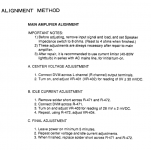
A) Yes, following the attached repair guideline, both output transistor collectors need to be directly connected to the 43V supply rails in order to set bias current correctly. That's what the solder bridges do but only for the positive rail, collector side in either channel. I've never needed to do this and uncertain if any damage would occur if you didn't. Perhaps other can help there......the thought does occur that I'm going in an unending circle and that replacing everything with a potential to fail might work.
If I do this, before turning on power afterwards, would it be wise to:
A) reconnect the solder bridge of resistors R471 & R472?
B) replace the non-TO92 transistors too (like the Darlingtons) as I got duplicates?
C) put a 100W bulb in the DBT or eliminate it and go for straight AC?
Earlier I mentioned having concerns about bias pots VR403 & VR404.....
B) I doubt these transisstors will need replacement as they should not be active until an input signal peak is high enough to require >43V rails. The voltages elsewhere in the amplifier should be OK without them and since there was voltage across them (C-E) on your last tests, I assume they are OK.
C) No, always use as low a power bulb as necessary to maintain a comfortably low supply voltage that still keeps the circuits operational. That is, they have a sufficient voltage across the junctions to operate normally. I can't say what that should be for the BD681/2 but the 60W bulb seemed to be sufficient, according to the supply rails measured.
I can't help with parts availability but I now use "sealed" cermet pots as replacements and they are available in a range of small small footprint sizes, from several manufacturers. Unfortunately, local suppliers just can't keep the inventories necessary to service so many different consumer products out there, some going back 40 years and more. This example stocked by Digi-key has 5mm x 2.5mm pitch leads - perhaps small enough: 3362P-1-102LF Bourns Inc. | Potentiometers, Variable Resistors | DigiKey.
If you remove a pot, switch or other mechanically operated device for cleaning, take the opportunity to test its function out of circuit with your meter, wiper to either end terminals, as you operate it slowly.
OK, the 60W stays. The electrolytic capacitors I intend to replace are in my possession and I have a reasonable supply of KSC1845/A992. I also picked up some of those cermet pots 10K & 1K. Funny but previously when I went looking for new pots, I saw blue ones exactly as in your photo but passed on buying them. I obviously did not pay close enough attention because through the plastic bag each was contained in, it looked to me like they had 4 legs not 3.
I will probably get started tonight doing all the re & re's but it will take me a few days of picking away at it as time allows. I will not apply any power until all the new parts I have are in place.
With that in mind, is there a specific place to have my test leads connected at first start up? Whether or not doing it has any benefit at all, I'm not qualified to say but I thought that bring able to see meter reading immediately upon turn on would be useful.
Regarding those solder bridges again. I removed them quite some time ago and they remained disconnected ever since. Any chance that their absence has been the cause of the voltage anomalies?
A trick I learned quite early on was to remove output transistors and feedback VAS or driver output back into LTP temporarily.
This makes likelihood of blowing components much less problematic.
You can prod around the VAS and driver stage with the unit powered up.
This makes likelihood of blowing components much less problematic.
You can prod around the VAS and driver stage with the unit powered up.
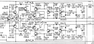
The solder bridges just short R471 (in this snip of the left channel) which otherwise is in series with the low voltage supply rail. I think that with some types of problem in the main output section of the power amplifier (2SD1047/B817), that 1 ohm resistor would then burn, removing the + low voltage supply rail connection. The variable high voltage rail is connected via Q431 and if that or its control circuit to the right side of it are dead, you would then not have any + rail voltage at all......Regarding those solder bridges again. I removed them quite some time ago and they remained disconnected ever since. Any chance that their absence has been the cause of the voltage anomalies?
Your previous posts indicate you do or did have the low and high + voltage supplies there, at the collector of Q427 and the emitter of Q431 respectively.
As you can see from the service manual's alignment procedure, the only purpose of the solder bridges is to enable correct bias setting. After replacing any semis in the output stage, you have to readjust the bias current anyway, for all linear power amplifiers. In this case you would then remove the bridges as directed, assuming you could do that successfully. I don't see any reason beyond that to resolder them.
Attachments
Last edited:
Sorry, timed out again - Note: the reverse is true and the bridges are normally in place, so yes, resolder if the bias current is adjustable and within the ballpark of correct setting.
The temptation for rest was too great this week so i did not touch this receiver again until today.
I will outline what I've done but note that the solder bridges are still not established. Maybe wrongly, but I assume from your explanation that other than the main output transistors, it makes no difference elsewhere on the board. If and when the power amp voltage problems are corrected, I would set the bias and then re-solder the bridges making it the very last thing.
Today I replaced all electrolytic capacitors in the affected channel.
Also replaced again TO92 transistors Q401/402/405/406/409/413/415 with fresh KSC1845's and KSA992's.
Bias adjust pots VR403/404 replaced with new 1K
Center voltage adjust pots VR401/402 (needed or not) replaced with new 10K.
There are four TO92 transistors I have not touched at all - Q301/302 (2SK363 FET) & Q501/502 (2SC1815 GR NPN). If these could be playing a role in the power fault, I have a few 2SC1815's (probably not GR) on hand but not the other. If you think I should replace these, please advise. As mentioned, I have 2SC1815's but will obtain 2SK263's or whatever may be a current substitute.
If the above transistors are a non-factor, I can go ahead with powering up but I'm a little gun shy. Perhaps something else is amiss and damage will reoccur? Assuming no sparks, smoke, loud noises or brightly lit DBT, please remind me again where I should be checking for voltage - Vbe's all around or maybe first measure across R471/472 to see if any idle current is there?
Q501/502 are regulator transistors for the +/-20V power supplies to opamps in the tone control/preamp section and to power indicator LEDs 501,502, 502-2. However, you only have to verify that you do have around +/- 14V at IC301 pins 8,4 to know they are fine.
JFETs Q301/2 act as muting switches for the preamp output so shouldn't be relevant at this point.
For taking care, it would not hurt to short out or at least fit 1K resistors across the main amp input sockets to ensure there is no or very little spurious input DC in play. I would measure if there was anything detectable there and quite early on the check list.
The preamp and main amps are internally connected so as long as the muting JFETs work (that is, conduct the preamplifier signal to the main amp) there could be input to the power amp but it's no problem to simply bypass the preamp and connect a known signal (with a volume control to prevent a blast of full power) to the main in sockets. The tape monitor switch also provides a preamp bypass loop which is useful if you suspect problems there but that's unnecessary for the moment.
Shotgunning really doesn't help - it's desperation when you can't follow circuits and derive the expected voltages logically. I'm guilty of it too when I'm stumped but I can't recall too many times that it ever worked for me. The clues are in the blown parts and that's why it's necessary to check them out systematically and record the results, as in how it was when you began. At one time I would photocopy parts of the schematic and highlight the fault paths and components in various colours to get a visual from the mess of numbers - mainly because I just couldn't juggle it all in my head - Unhelpful advice but sometimes a little sympathy is all it takes.
As far as key checkpoints go, DC voltage at the output node is always the priority - it should be zero but never exactly is with an unadjusted amplifier. If it really is zero before setting, things could actually be grim instead. Something to be careful of with NAD designs from the era of the original 3020 design - the output protection is essentially just a PCB mount circuit breaker, like you press to reset on the back of some old appliances and stage equipment, only no reset button here, just wait 'til the bimetal strip cools and it self-resets. Crude and it works if only tripped occasionally but being slow acting, damage is inevitable on a larger amp like this one. May not be a problem but comparing output voltage before BK-1,2 and after (at the output terminals) as a check on the actual output voltage, would be a fair indicator of their condition.
Only when you measure the output as within a few volts of zero, can you proceed to check much else though. You would then have to track down likely causes of a substantial offset and just what to check would depend on what you find wrong according to marked voltages. If reasonably close you should then check Vbe and if suspect, check for shorts again.
- Status
- Not open for further replies.
- Home
- Amplifiers
- Solid State
- NAD 7240pe - all output transistors failed?