I have found a 375 watt mosfet FQA90N15.
I reckon I can get 300WRMS out of a pair of these with +/- 55 volt rails.
They have quite a high gate capacitance but I think I can drive that ok with 100R gate resistors.
I reckon I can get 300WRMS out of a pair of these with +/- 55 volt rails.
They have quite a high gate capacitance but I think I can drive that ok with 100R gate resistors.
An externally hosted image should be here but it was not working when we last tested it.
Only TO3P package - How are you going to cool them for linear use in class AB at that 300W output level?
https://www.fairchildsemi.com/datasheets/FQ/FQA90N15.pdf
https://www.fairchildsemi.com/datasheets/FQ/FQA90N15.pdf
Last edited:
the maximum reliable outpu is roughly 1/4 of the toatl output device Pmax.
Two 375W devices should give a reliable 190W, if you can keep them within your Tc design limits.
Two 375W devices should give a reliable 190W, if you can keep them within your Tc design limits.
Last edited:
Hi Guys
FQA90N15 is optimised for switching but has a huge DC safe operating area. Check that the waste heat falls within that area and you are good to go. To make full use of the Pd might require liquid cooling - most super mosfets do.
Gate capacitance is pretty high so you might want to add an EF driving it directly.
At 56V rails I assume you are thinking 4R load? This requires 49V peak drive for 600W, but it is unlikely the supply will stay at 56V nor that a 7V margin will be sufficient for gate voltage. You might need a boosted positive rail. The good thing is that at half the supply voltage across the load, waste heat is <200W peak. There is hope.
Have fun
Last edited:
I have done a few calculations on the circuit.
Worst case power dissipation is at 36 volts sine wave across 4 ohm speaker with 55 volts B+. This gives 9 amps * 19 volts across transistor = 171 watts.
Then given transistor is only on for 50% of time the dissipation is quite low.
Worst case power dissipation is at 36 volts sine wave across 4 ohm speaker with 55 volts B+. This gives 9 amps * 19 volts across transistor = 171 watts.
Then given transistor is only on for 50% of time the dissipation is quite low.
Hi Guys
Nigel: Your drawing showed 56V so at 28V across the load and 28V across the mosfet, power in each is 196W at 4R. Over here 196 is greater than 171... new world math vs old world math?
As a bass amp or so two devices might be sufficient. As you know, there are tonnes of advantages to using parallel devices if you want low THD20 especially. But overall I think it is worth trying.
Have fun
Hi Guys
Over here 196 is greater than 171... new world math vs old world math?
Have fun
If you just take a steady DC voltage then your calculation is right.
I used a sine wave modelled in a PC program to plot the power in transistor and in speaker.
This is why my averaging reading over a sine cycle is less.
=======================================================
private void runclick(object sender, EventArgs e)
{
int cx;
int bplus; //60 volt rail
int ax,bx,dx;
int loadpower;
int tranpower;
int bplus2;
int speakerimpedance;
string str;
str = "";
loadpower=0;
tranpower = 0;
bplus = 55; //60 volts bplus rail
speakerimpedance = 4;
for (bplus2 = 0; bplus2 <= bplus; bplus2++)
{
for (cx = 0; cx <= 360; cx++)
{
/////////////////
//calc power into load
/////////////////
ax = (sindx(cx) * bplus2) / 255; //get voltage across load
ax = abs(ax); //only work with +ve voltages else cancels to zero
loadpower = loadpower + (( ax * ax) / speakerimpedance); //volts squared div 4ohms
///////////////////////////
//calc power in transistor
///////////////////////////
bx = (sindx(cx) * bplus2) / 255; //get voltage across load
bx = abs(bx);
bx = bx / speakerimpedance; //div by speakerimpedance to get current through load
dx = (sindx(cx) * bplus2) / 255; //get voltage across load
dx = bplus - abs(dx); //bplus - volts across load = volts across transistor
//get power in transistor
tranpower = tranpower + (dx * bx); //v * i
}
loadpower = loadpower / 360;
tranpower = tranpower / 360;
str = str + "Voltage=" + Convert.ToString(bplus2) + " Loadpower=" + Convert.ToString(loadpower) + " Tranpower=" + Convert.ToString(tranpower);
str = str + "\n";
}
//System.Windows.MessageBox.Show("Load power=" + Convert.ToString(loadpower));
//System.Windows.MessageBox.Show("Transistor power=" + Convert.ToString(tranpower));
Form2 form2 = new Form2();
form2.richTextBox1.Text = str;
form2.ShowDialog();
}
Last edited:
What 375W/250W/115W/whatever *actually* means is that it will just melt/short dissipating that power if and only if you can keep device flange temperature at 25C .
It only describes chip to flange thermal resistance.
Mind you, flange-to-any heat sink , even if a pure aluminum asteroid 1 km in diameter will be definitely > 0 C/W so not even said asteroid is enough even if it's at 25C
Which then means that even such a huge heatsinking mass should be kept way below 25C for the 375W rating to apply.
Not even liquid cooling would be enough, nor the largest fan on Earth, unless liquid/gas is well below 25C ... would you be surprised at minus 65C or lower?
My point is that seat of the pant estimations such as
Might apply in some cases (basically by chance), in no way can be extrapolated.
Now a little Math.
Datasheet shows:
so for a 25C aluminum asteroid we can dissipate (175-25)/0.64=235W
........... now we are *starting* to talk
of course, that's *destruction* temperature and a million Tons of aluminum might get a little expensive, so let's set somewhat more realistic goals ... and add a little safety margin.
Just because I'm writing this and I'm in total control of this keyboard (insert mad scientist laughter here 😉 ) I suggest:
140C max junction temperature (35C below meltdown)
35C max ambient temperature (just 10C above "human comfortable temperature")
90C max heatsink body temperature (just 10C under third degree human skin burn damage)
mind you, these are usable but scorching temperatures.
so now we have (per device):
(140-90)/0.64=78W per device
use that for whatever you need , that is a realistic value.
I don't state how you avoid your heatsink to surpass 90C , it's up to you, not the main point here.
Can you make a 300W RMS Class AB amplifier with a total 156W dissipation capability? (2 devices)
Yes, seems entirely feasible, not a big deal.
Does this match the "rated device dissipation" P/4 estimation?
It might ... it might not ... only standard thermal calculation as shown above can say for sure.
Main point is that "datasheet" device dissipation is just a nice way to spec Rth ; beyond that it's up to the designer.
Of course: "look MA !!!!! three-hundred-and-seventy-five-watts with a single transistor !!!!!!!!!! " definitely sounds (and looks) good 😉
FWIW I remember very old ads (think late 70's) about first high power rack amps available (think 150/200 W per channel) stating something like: "powered by 1000 Watts total transistor dissipation" ... which if nothing else was a way to print the magical word "1000 Watts" in the ad copy .
Oh well 🙂
It only describes chip to flange thermal resistance.
Mind you, flange-to-any heat sink , even if a pure aluminum asteroid 1 km in diameter will be definitely > 0 C/W so not even said asteroid is enough even if it's at 25C
Which then means that even such a huge heatsinking mass should be kept way below 25C for the 375W rating to apply.
Not even liquid cooling would be enough, nor the largest fan on Earth, unless liquid/gas is well below 25C ... would you be surprised at minus 65C or lower?
My point is that seat of the pant estimations such as
are meaningless on their own merit.the maximum reliable outpu is roughly 1/4 of the toatl output device Pmax.
Might apply in some cases (basically by chance), in no way can be extrapolated.
Now a little Math.
Datasheet shows:
Thermal Characteristics
Symbol ---------- Parameter --------------------------------- Unit
RθJC --- Thermal Resistance, Junction-to-Case, --- Max. 0.4 °C/W
RθCS --- Thermal Resistance, Case-to-Sink, --------Typ. 0.24 °C/W
so for a 25C aluminum asteroid we can dissipate (175-25)/0.64=235W
........... now we are *starting* to talk
of course, that's *destruction* temperature and a million Tons of aluminum might get a little expensive, so let's set somewhat more realistic goals ... and add a little safety margin.
Just because I'm writing this and I'm in total control of this keyboard (insert mad scientist laughter here 😉 ) I suggest:
140C max junction temperature (35C below meltdown)
35C max ambient temperature (just 10C above "human comfortable temperature")
90C max heatsink body temperature (just 10C under third degree human skin burn damage)
mind you, these are usable but scorching temperatures.
so now we have (per device):
(140-90)/0.64=78W per device
use that for whatever you need , that is a realistic value.
I don't state how you avoid your heatsink to surpass 90C , it's up to you, not the main point here.
Can you make a 300W RMS Class AB amplifier with a total 156W dissipation capability? (2 devices)
Yes, seems entirely feasible, not a big deal.
Does this match the "rated device dissipation" P/4 estimation?
It might ... it might not ... only standard thermal calculation as shown above can say for sure.
Main point is that "datasheet" device dissipation is just a nice way to spec Rth ; beyond that it's up to the designer.
Of course: "look MA !!!!! three-hundred-and-seventy-five-watts with a single transistor !!!!!!!!!! " definitely sounds (and looks) good 😉
FWIW I remember very old ads (think late 70's) about first high power rack amps available (think 150/200 W per channel) stating something like: "powered by 1000 Watts total transistor dissipation" ... which if nothing else was a way to print the magical word "1000 Watts" in the ad copy .
Oh well 🙂
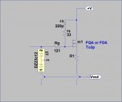
Nigel,
The Fairchild FQA (and FDA) series of mosfets will work for audio amplifiers, but ONLY if you use a gate/drain snubber (see diagram). Without the snubbers they WILL burst into oscillation and destroy themselves quite quickly. The values on the diagram are a good starting point.
I suggest you use 1206 size smd components for Cs and Rs, and that you make the gate resistor (Rg) a low power resistor (1/8 watt or 1206 or 1210) so that if the mosfet does decide to fail, the gate resistor will quickly fail and save the rest of the circuit. Keep the track lengths between the gate and the Rs and Rg resistors small (ie 5mm).
There are a number of suitable for audio mosfets FQA32n20c, FQA36p15 for complimentary, and FQA40n25, FQA46n15, FDA69n25. The Fairchild models are basically useless.
I haven't tried these in a Quasi configuration, so good luck.
Regards,
Paul Bysouth
Attachments
Hi Guys
Paul:
"There are a number of suitable for audio mosfets FQA32n20c, FQA36p15 for complimentary, and FQA40n25, FQA46n15, FDA69n25. The Fairchild models are basically useless."
The statement seems contradictory as all the devices are Fairchild, but you say they are good then you say they are bad?
Have fun
the maximum reliable outpu is roughly 1/4 of the toatl output device Pmax.
Two 375W devices should give a reliable 190W, if you can keep them within your Tc design limits.
Usually for mosfet devices 1/3 of max power are sufficient for reliable operation, i use 2 couple of FDA69N25 (TO3P package) @ +/- 70 volts into 4 ohm (rms sine wave) since 2 years with no trouble in PA application, generous active heatsink is mandatory, in musical test they can handle 2 ohm load
Kevin,
Paul and I have tested most of them....... he is correct; the models are not refined at all.
Hugh
Paul and I have tested most of them....... he is correct; the models are not refined at all.
Hugh
Nigel,
The Fairchild FQA (and FDA) series of mosfets will work for audio amplifiers, but ONLY if you use a gate/drain snubber (see diagram). Without the snubbers they WILL burst into oscillation and destroy themselves quite quickly. The values on the diagram are a good starting point.
I suggest you use 1206 size smd components for Cs and Rs, and that you make the gate resistor (Rg) a low power resistor (1/8 watt or 1206 or 1210) so that if the mosfet does decide to fail, the gate resistor will quickly fail and save the rest of the circuit. Keep the track lengths between the gate and the Rs and Rg resistors small (ie 5mm).
There are a number of suitable for audio mosfets FQA32n20c, FQA36p15 for complimentary, and FQA40n25, FQA46n15, FDA69n25. The Fairchild models are basically useless.
I haven't tried these in a Quasi configuration, so good luck.
Regards,
Paul Bysouth
Thanks for the advice.
I have added snubbers as you suggest to pcb.
I also found the gate resistors were miles away from the mosfets, I have moved them as close as possible.
The statement seems contradictory as all the devices are Fairchild, but you say they are good then you say they are bad?
'The map is not the territory' - he's talking about the simulation models, not the devices themselves.
Only TO3P package - How are you going to cool them for linear use in class AB at that 300W output level?
https://www.fairchildsemi.com/datasheets/FQ/FQA90N15.pdf

Notice how the derating drops the Pd as temp rises. In a linear audio situation, when the speaker becomes reactive and dumps current into the output stage when significant Vds occurs, the instantaneous die temperature soars quickly, this being on top of a higher than ambient initial temperature due to operation, and being cranked up. 2.5W/C. So at a die temp of 150C, you got about 62W of dissipation. That is pretty hefty at that temperature but 300Wave from one pair is pushing it for maximum abuse operation. Full range audio might be OK due to the effectively short duty cycle, peak to average ratio.
Class A perhaps?
The pcb's arrived today.
The amp sounds good.
Found a mistake on my bridging circuit, I was getting a large DC offset on its output. Seems the LTP was pulling down the input a bit and upsetting the bridge circuit. I added a coupling capacitor to the bridge circuit and that fixed the problem.
The output dc offset moves around a bit but not too much.
I added a DC speaker protect circuit to the pcb, that works fine.
I was advised to add snubbers to the output mosfets.
The amp seems to work fine without but I might add them anyway.
An externally hosted image should be here but it was not working when we last tested it.
I found what was wrong with the DC offset.
The bias current was too low and allowing the output dc to move around a bit.
I set the bias to just eliminate crossover distortion and that seems to work well.
The bias current was too low and allowing the output dc to move around a bit.
I set the bias to just eliminate crossover distortion and that seems to work well.
I found what was wrong with the DC offset.
The bias current was too low and allowing the output dc to move around a bit.
I set the bias to just eliminate crossover distortion and that seems to work well.
I found on the LTP I am getting -1.5 volts at idle.
I think this has been upsetting the feedback electrolytic capacitor.
I reversed it to stop negative volts across it.
Nigel,
The Fairchild FQA (and FDA) series of mosfets will work for audio amplifiers, but ONLY if you use a gate/drain snubber (see diagram). Without the snubbers they WILL burst into oscillation and destroy themselves quite quickly. The values on the diagram are a good starting point.
Regards,
Paul Bysouth
I am not getting any oscillation without the snubbers.
I did to start with but I had not set the bias up correctly or fitted the zobel network.
I have tried it under varying loads and amplitudes and it works ok.
- Home
- Amplifiers
- Solid State
- 300 watts RMS out of 2 mosfets ?