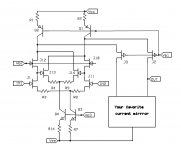
A while ago Bob Cordell mentioned using the cascomp technique with JFET’s but I don’t think any actual circuit was shown. Since I was thinking of playing with some very open loop linear circuits I put this together as a test of the concept (simulation). I pick some arbitrary but reasonable values and used K74/J170 type devices in the signal path. The current sources are not critical and there are many reasonable choices.
This is a differential in current conveyor and the transconductance is set by R3 + R8 which I chose at 1K. The cascomp circuit removes the effect of the source voltages of the input devices (J1, J11). This is achieved by sensing the differential voltage on the cascode device’s sources (J10, J12) with J13 and J14, and if R4 + R9 is equal to R3 + R8 the cross-coupled output currents will subtract the error due to J1 and J11’s source voltage which includes the square law non-linearity. In practice R4 and R9 are slightly smaller than predicted and can be trimmed to a very good distortion null (J1, J11, J10, and J12 are assumed the same type of devices). Note: at null the transconductance is exactly 1K since the linear portion of the source voltages is also removed.
In simulation the result is probably better than one could reasonably expect (~1ppm) for a full 5v p-p input range. This is with J1 and J11 at 5mA, J13 and J14 at 1mA, and the upper current sources at 10mA. This would be +-2.5mA of current out of the OUT node for +-2.5V on the input. The input can be used differential or single ended of either polarity making it very versatile. In practice it should be easy to achieve -90dB or more open loop voltage to current transfer linearity.
There is a noise penalty and with care and large supply voltages to get lots of degeneration on the current sources the above values can get ~6.8nV/rt-Hz which would be good in a line-stage or PA. This circuit is shown as an input stage to an op-amp but it could be a building block for little or no feedback amplifiers too.
Attachments
I recommend that you replace the AD825 jfet front end with this!
Well you could integrate this but the common mode headroom from all those Vp's suffers and no one will buy a general purpose amp with 30mA of supply current anymore.
But, there is no BW variation at all with differential input so no possibility of PIM. 🙂
Scott, before I look into an outright theft of this front end, how sensitive is it to FET matching?*
*in units of milliWurcers, of course!
*in units of milliWurcers, of course!
Last edited:
I was wondering the same thing: would seem that you also want very good matching of r3-r8 and r4-r9 pairs (art least to themselves.
Parallel jfets should help with ensemble values, though.
Parallel jfets should help with ensemble values, though.
Complementary JFETs and complementary BJTs all on the same die?Well you could integrate this but the common mode headroom from all those Vp's suffers and no one will buy a general purpose amp with 30mA of supply current anymore.
BTW how about turning the PJFET cascodes into Richard Jaeger super ro cascodes, by connecting J3gate to Q2emitter and connecting J4gate to Q1emitter? Citation in IEEE JSSC
Scott, before I look into an outright theft of this front end, how sensitive is it to FET matching?*
*in units of milliWurcers, of course!
I'm not sure the matching needs to be obsessive, I am taping out a board to see. A couple of simple judiciously placed trim pots could make all the difference (i.e. maybe offset and THD). BTW use at will.
Anyone's favorite embellishments are always welcome, this is just the basic outline.
Complementary JFETs and complementary BJTs all on the same die?
BTW how about turning the PJFET cascodes into Richard Jaeger super ro cascodes, by connecting J3gate to Q2emitter and connecting J4gate to Q1emitter? Citation in IEEE JSSC
The folded cascode does not really need PFET's the base current errors using pnp's are secondary. Of course the Gothic buttresses could be added to reduce the errors. This is an old in joke, at a design review someone commented that a schematic with cascodes and second order base current corrections added looked like a Gothic cathedral with all the flying buttresses.
- Status
- Not open for further replies.
- Home
- Amplifiers
- Solid State
- A cascomp (ultra-linearized) circuit with JFET's