Intro: This is an extension of this thread, whose author suggested I start, as subject matter has moved from discussion stage to design stage.
http://www.diyaudio.com/forums/analogue-source/289153-mc-phono-amp-first-stage.html
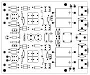
Here is the latest schematic and board layout. The board is 4.7in X 3.9in designed to slide into a standard Hammond enclosure. It employs the ubiquitous 3.5mm trs jack for both input and output. If needed, cables that go from these to XLR are readily available at pro audio sites, not to mention ebay. I have installed 3.5mm jacks at the turntable, connected directly to the wires from the tonearm. Still some tweaking to do, should have one operating in a couple of weeks.
http://www.diyaudio.com/forums/analogue-source/289153-mc-phono-amp-first-stage.html
Here is the latest schematic and board layout. The board is 4.7in X 3.9in designed to slide into a standard Hammond enclosure. It employs the ubiquitous 3.5mm trs jack for both input and output. If needed, cables that go from these to XLR are readily available at pro audio sites, not to mention ebay. I have installed 3.5mm jacks at the turntable, connected directly to the wires from the tonearm. Still some tweaking to do, should have one operating in a couple of weeks.
Attachments
Last edited:
Thanks for starting this thread Polyphaze. I have wanted to build a balanced phono stage for some years now, but I have never been able to work out a design that satisfies me. The Phobos looks just perfect for my needs and I will be building this up ASAP.Intro: This is an extension of this thread, whose author suggested I start, as subject matter has moved from discussion stage to design stage.
http://www.diyaudio.com/forums/analogue-source/289153-mc-phono-amp-first-stage.html
Here is the latest schematic and board layout. The board is 4.7in X 3.9in designed to slide into a standard Hammond enclosure. It employs the ubiquitous 3.5mm trs jack for both input and output. If needed, cables that go from these to XLR are readily available at pro audio sites, not to mention ebay. I have installed 3.5mm jacks at the turntable, connected directly to the wires from the tonearm. Still some tweaking to do, should have one operating in a couple of weeks.
I will be running off +/-24 volt rails ( 4 x 12V SLA batteries) so circuit values may be different to yours. Are you able to update your circuit with all values so I can work through the values I will need.
Regards
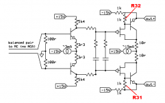
I would like to ask about resistors R31 and R32 (labeled in the attached schematic).
The voltage across each of these resistors is VBE, about 0.7 volts.
If their resistance is 1000 ohms, the current in each of these resistors is about 0.7 milliamperes.
So the drain current of the Pchannel JFETs is about 0.7 milliamperes.
The total current per side is 7.5 milliamps (15mA / 2). The PJFET gets 0.7 mA and the NPN gets 6.8 milliamps.
That is what I would to ask about. The current in the NPN is about 10 times larger than the the current in the PJFET. Why? Why this particular 10-to-1 ratio? Why not 2-to-1, or 1-to-1, or any other ratio?
Thanks for your time!
Attachments
I dont know. I'm a bit new to jfets. It just looks good in a sim. What do you suggest?
Hopefully Hazard500 will chime in.
Hopefully Hazard500 will chime in.
Thanks for starting this thread Polyphaze. I have wanted to build a balanced phono stage for some years now, but I have never been able to work out a design that satisfies me. The Phobos looks just perfect for my needs and I will be building this up ASAP.
I will be running off +/-24 volt rails ( 4 x 12V SLA batteries) so circuit values may be different to yours. Are you able to update your circuit with all values so I can work through the values I will need.
Regards
It seems that no changes whatsoever are required to run with 24V rails. However, in the output stage, one could increase the CCS current, and decrease the R of the output load resistors, thereby lowering the output Z, a good thing.
Last edited:
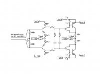
Hi Mark, my simulator (SIMETRIX) doesn't have models for the exact components we use, but using generic devices I have tried out a few scenarios. What I observe is that, for a fixed current, the more current that gores through the BJT the higher the gain. Now we need enough current to turn on the fet, and keep it turned on for the full voltage swing of the first stage. The 2SJ74 fets I have measure Vgs of 300 to 400mV for drain current of 1mA, and this seems a reasonable figure. This implies that the drain resistors should be about 700ohm (but it would also be worthwhile measuring Vbe of the BJT at collector current of 7mA to check this figure. In fact I think you need to measure Vbe and match the BJTs for this to ensure that jfets get equal current for equal drain resistors.)I would like to ask about resistors R31 and R32 (labeled in the attached schematic).
The voltage across each of these resistors is VBE, about 0.7 volts.
If their resistance is 1000 ohms, the current in each of these resistors is about 0.7 milliamperes.
So the drain current of the Pchannel JFETs is about 0.7 milliamperes.
The total current per side is 7.5 milliamps (15mA / 2). The PJFET gets 0.7 mA and the NPN gets 6.8 milliamps.
That is what I would to ask about. The current in the NPN is about 10 times larger than the the current in the PJFET. Why? Why this particular 10-to-1 ratio? Why not 2-to-1, or 1-to-1, or any other ratio?
Thanks for your time!
So, there is no magic ratio as far as I can tell, but I intend to start with fet current of 1mA and see how we go.
OK that seems OK - but you haven't included the values for the components in the eq network. What would these be?It seems that no changes whatsoever are required to run with 24V rails. However, in the output stage, one could increase the CCS current, and decrease the R of the output load resistors, thereby lowering the output Z, a good thing.
Thanks, Hazard
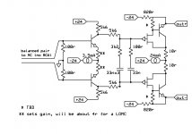
Thanks Poly, I've been playing around with this in SIMETRIX. I found some spice models for MAT02, and 2SJ74, so hopefully the simulation is pretty close to real life - its certainly very different to the outputs when I used generic devices. I have included both the circuit diagram and response curve. For inpuy of 0.5mV, output is around 2.5V @ 1kHz, so gain is just about right for ZYX and Denon, with a little overhead if real life circuit doesn't meet simulated results.Here is an updated schematic, optimized for 24V rails and adding some component values.
Note I have used +24/-12V rails. This helps to keep load resistors on the output stage, which define output impedance, as low as possible. Current in 2SJ74 is now 2mA, I need to check matching on my devices (which was done at 1mA). I will build this and test when I receive MAT02, due in today's mail.
Attachments
Last edited:
Thanks Poly, I've been playing around with this in SIMETRIX. I found some spice models for MAT02, and 2SJ74, so hopefully the simulation is pretty close to real life - its certainly very different to the outputs when I used generic devices. I have included both the circuit diagram and response curve. For inpuy of 0.5mV, output is around 2.5V @ 1kHz, so gain is just about right for ZYX and Denon, with a little overhead if real life circuit doesn't meet simulated results.
Note I have used +24/-12V rails. This helps to keep load resistors on the output stage, which define output impedance, as low as possible. Current in 2SJ74 is now 2mA, I need to check matching on my devices (which was done at 1mA). I will build this and test when I receive MAT02, due in today's mail.
OK, good progress. That response curve is very cool.
I was puzzled at first by your move to a -12V rail, but realized you must be looking for gain, as 74db is a lot more than I have ever needed. However, increasing gain is much better done by decreasing the emitter (source) resistors. So lets go back to -24V rail, decrease R11 R12 to 6r, decrease output resistors to 1k, and up the source current to 30ma. The circuit should now have the same gain profile, but with lower output Z and headroom galore. In fact, with an overload input of 5mv, output will be a very clean 25V with room to spare!
BTW, I'm leaning toward all BJTs in my implementation. No particular technical reason, I'm just a bit out of my comfort zone working with jfets.
You should probably try them in your sim, if just for a reference.
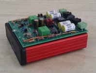
OK, the deed is done. Here are a couple of pics, and schematic, of Phobos 2.0. After several several hours of listening, I can say that it is a marked improvement over the original, which was already quite nice IMO.
You are right Hazard, 24V is a bit too hot for this output stage. I went with 15V because that was easiest for me, 12V or anything in between is fine.
There is an offset in this first build, hence the output caps remain. With more careful component matching, and better regulation, I'm pretty sure the caps can be dispensed with next time.
I'm going to send a pm with some other details.
Attachments


OK, the deed is done. Here are a couple of pics, and schematic, of Phobos 2.0. After several several hours of listening, I can say that it is a marked improvement over the original, which was already quite nice IMO.
You are right Hazard, 24V is a bit too hot for this output stage. I went with 15V because that was easiest for me, 12V or anything in between is fine.
There is an offset in this first build, hence the output caps remain. With more careful component matching, and better regulation, I'm pretty sure the caps can be dispensed with next time.
I'm going to send a pm with some other details.
Looking nice Polyphaze. One question - is CCS in output stage really 30mA? based on values shown, this implies about 1mA in the pnp device and 14mA in the npn device. What is dissipation in this device? I can see that the purpose of this current is to keep the load resistors (and hence output impedance) low, but I am surprised to see 14mA in one transistor.
I have been continuing to explore the complementary feedback pair as a fet/bjt pair. Tot test this further I have implemented a standalone CFP as a gain stage for my strain gauge pre-amp. See this attachment for a description of the circuit.
http://www.diyaudio.com/forums/analogue-source/211081-strain-gauge-jfet-pre-amp-2.html#post4682324
Now the strain gauge circuit is based on n-jfet and pnp bjt. To build the Phobos I will need p-jfet and npn bjt. I have been matching 2sj74 and have a few matched pairs so that's good. Also, I bought a MAT02 and LM394 from a local ebay seller. I intend to use the MAT02 in the input stage of the phobos, and use the LM394 as the bjt in the CFP output. What do you think? Based on the success of the strain gauge circuit, I am confident that this should work OK.
The CCS is 30mA. The quiescent Vce of the npn bjt is around 8V, so dissipation is about 1/8 watt, easy enough for a T92 package.
The LM394 looks like a great choice. I didn't know about them.
I found your strain gauge project most interesting. I know what a strain gauge is, but I had never heard of one being used as a phono transducer.
Last edited:
Polyphaze, I've just read an old application note for LM194/LM394 transistors (these are, i believe, the preferred low noise device prior to introduction of MAT02).OK, the deed is done. Here are a couple of pics, and schematic, of Phobos 2.0. After several several hours of listening, I can say that it is a marked improvement over the original, which was already quite nice IMO.
You are right Hazard, 24V is a bit too hot for this output stage. I went with 15V because that was easiest for me, 12V or anything in between is fine.
There is an offset in this first build, hence the output caps remain. With more careful component matching, and better regulation, I'm pretty sure the caps can be dispensed with next time.
I'm going to send a pm with some other details.
http://www.ti.com.cn/cn/lit/an/snoa626b/snoa626b.pdf
An interesting comment I just saw (Page 6 of the PDF):
"The single-ended amplifier shown in Figure 4 was designed for source impedances below 250Ω. At this level, the LM194 should be biased at 2.5 mA (or higher) collector current."
So, maybe we should think about a bigger CCS (5mA) for the MAT02, to optimise the noise performance of this stage?
The LM194 is a tighter spec version of LM394, and is preferred device if we can get it. I can see a few listings on eBay (China/HK) and my suspicion is that they will be fakes. What are your experiences with obtaining obsolete parts such as MAT02?
Regards, Hazard
Hi,
the That 300 series are actual replacement parts for the MATs, both the NPN and the PNP.
That also offers matched Quads and matched complementary Quads.
The Quads would allow for paralleling the input transistors, reducing noise even more.
As far as I remember are the LMs older designs and more noisy than the MATs and Thats.
jauu
Calvin
Hi Calvin, LM194 is old but still seems to hold up.Hi,
the That 300 series are actual replacement parts for the MATs, both the NPN and the PNP.
That also offers matched Quads and matched complementary Quads.
The Quads would allow for paralleling the input transistors, reducing noise even more.
As far as I remember are the LMs older designs and more noisy than the MATs and Thats.
jauu
Calvin
LM194. Input voltage noise, at 1mA, = 1nV.
MAT02. Input voltage noise @1mA = 1nV
THAT300B input noise voltage @1mA = 1nV
So noise performance is equal. However THAT series seems to offer less gain and matching is not quite as tight.
LM194 Hfe = 350 (min) 700 (typical). Hfe match = 0.5% (typical) 2% (max)
MAT02 Hfe = 500 (min) 605 (typical). Hfe match = 0.5% (typical) 2% (max)
THAT300B Hfe = 300 (min). Hfe match = 4% (typical)
I have heard (IIRC) that the transistors in THAT300 are on separate dies, not monolithic like LM/MAT, which explains relatively poor Hfe matching - do you now if this is right?
So LM194 appears to have good performance - as long as we don't but fakes!!
Hi,
the LM194 looked more interesting than I had in mind 😉
Unfortunately its an obsolete device
jauu
Calvin
the LM194 looked more interesting than I had in mind 😉
Unfortunately its an obsolete device
jauu
Calvin
..Now the strain gauge circuit is based on n-jfet and pnp bjt. To build the Phobos I will need p-jfet and npn bjt. I have been matching 2sj74 and have a few matched pairs so that's good. Also, I bought a MAT02 and LM394 from a local ebay seller. I intend to use the MAT02 in the input stage of the phobos, and use the LM394 as the bjt in the CFP output. What do you think? Based on the success of the strain gauge circuit, I am confident that this should work OK.
Given the signal levels in the output npn bjt, I can't see any material benefit of using exotics like MATs, let alone obsoletes. Hfe matched BC550s (or equivalent) is the solution I'm going to stick with for now.
Polyphaze, I've just read an old application note for LM194/LM394 transistors (these are, i believe, the preferred low noise device prior to introduction of MAT02).
http://www.ti.com.cn/cn/lit/an/snoa626b/snoa626b.pdf
An interesting comment I just saw (Page 6 of the PDF):
"The single-ended amplifier shown in Figure 4 was designed for source impedances below 250Ω. At this level, the LM194 should be biased at 2.5 mA (or higher) collector current."
So, maybe we should think about a bigger CCS (5mA) for the MAT02, to optimise the noise performance of this stage?
The LM194 is a tighter spec version of LM394, and is preferred device if we can get it. I can see a few listings on eBay (China/HK) and my suspicion is that they will be fakes. What are your experiences with obtaining obsolete parts such as MAT02?
Regards, Hazard
I've discovered that small changes of the input CC affects the output stage in strange and mysterious ways. I am loathe to tinker with it now, as everything seems to be just right. Anyway, that app note was about SE, probably doesn't apply here.
Another sub for the MAT02 is the SSM2212, which is readily available. Unfortunately it is SMT only. Don't know if my aging hands are steady enough for SMT, but I guess I'll have to try.
I have never tried to obtain obsolete parts, only substitutes. For this project I had a pair of MAT02s left over from a purchase many years ago.
Finally, don't overlook resistors as a noise source. I use low noise metal films from Vishay.
Last edited:
OK this makes a lot of sense, and its the way I should go.Given the signal levels in the output npn bjt, I can't see any material benefit of using exotics like MATs, let alone obsoletes. Hfe matched BC550s (or equivalent) is the solution I'm going to stick with for now.
........
Finally, don't overlook resistors as a noise source. I use low noise metal films from Vishay.
At this stage I am still keen to use p channel jfet in output stage, mainly because all my designs are fet based and I am used to working with them. I get that bjt is best device for the first stage, which sees a low impedance source (moving coil cartridge), but the second stage doesn't see a low source impedance so I assume that a fet will give better noise performance in this spot.
My local shop stocks standard metal film resistor, I will have to shop around for Vishay - what is a good source for Vishay?
Regards, Hazard
Sometimes my diy projects take a while to reach fruition. In contrast, this project only took me 5 months to complete.
I finished up building the Phobos circuit all bjt as proposed by Polyphase, better to stick with a proven circuit firstly then I can experiment with j-fets etc later on. I decided to stick with +24V/-12V rails so I can continue to use my existing SLA batteries for power supply. So I tweaked a few resistor values. But otherwise built it exactly as designed.
I sent my Lenco to the workshop a month ago to get it ready for the debut of the Phobos but it's still there. So I pulled my old AR turntable/ Rega arm combo out of storage. This lead to further delays - there is another thread on this forum about Rega arms, did you know that Rega arms don't support balanced output? I didn't know this, and spent a frustrating week testing my finished Phobos for non-existant faults - finally I had to re-wire the Rega arm.
The current turntable is far from state of the art, but with my Monster Alpha Genesis 1000 it is making a very nice sound. This cartridge is only 0.2mV, but there is oodles of gain, and with battery supply it is dead quiet. I don't think its quite as nice as my old VSE valve amp but it sure is a quiet in comparison. But I've been running the Phobos for one day only, I've had the VSE since 1988 and its had a number of mod.s. Give me time to get to know the Phobos better, and we will see where we go.
As with my Strain Gauge pre-amp, the output stage is transformer coupled (Lundahl 1527XL). I have a variable resistor across the output of the transformer (its actually a series switched attenuater from eBay). Changing the resistance changes gain, my preamp is a selector switch so I am going from the output of the Phobos directly to power amp input. And its sounding great.
There has been quite a few phono pre-amps on diyaudio lately. But not many are balanced like the Phobos (actually I can't recall seeing any others). And it \\the Phobos sounds so good, I don't have any desire to or need (or indeed the time) to try other circuits). Thank you Polyphsae for a brilliant design, I am very happy with my pre-amp. Can't wait to get the Lenco back and hear it working with a 'proper' turntable.
- Status
- Not open for further replies.
- Home
- Source & Line
- Analogue Source
- PHOBOS, a balanced MC phono stage