Scott, I've been working on a FET phono stage which could be amenable to that approach (it costs all of two trimpots, such complexity!). Is there an advantage to having the trimmer be between the two current-setting resistors as opposed to having on fixed and one variable current setting resistor?
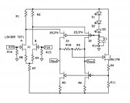
I wouldn't think so, last night I started cobbling together an all FET one stage differential amp based on the classic CMOS folded-cascode with common mode feedback. VERY rough sketch below. I have not looked, but have you seen this before?
I even simmed it with a 46dB RIAA network across the outputs (you need some buffers since the network was at 160k Ohms DC). I made the appropriate resistors trimmable so I could experiment. All you need to do is tap the main (160k) resistor in the middle to get the common mode feedback point. With a little care you can get 30V p-p out on 15V rails before clipping and nothing pathological happens at clipping.
Attachments
Last edited:
Where are you doing the trimming?
FWIW, I think I saw something like this from Norm Thagard. But it's been some years and I may be misremembering.
FWIW, I think I saw something like this from Norm Thagard. But it's been some years and I may be misremembering.
Where are you doing the trimming?
In this case R1/R2 and R5/R6. There are no source R's in the one I am trying. I would use the new LSK844 like Bob did for MM/MI cart. On second look the swing is closer to 20V p-p on 15V rails. Of course a current source on the input and better biasing could be added but I want to see how the trims work out.
I'll use "finger" warming on the input pair as a rough measure of drift and then see if offset and second harmonic has a pair of trims to eliminate both.
Remember the thing I tried before had N and P complementary inputs, this is very much an experiment. On second thought not having the source resistors to trim along with R1/R2 I might not be able to do what I want, you should probably wait for me to fiddle around a little.
Last edited:
My circuit is topologically different, but still relies on each side being well matched, n and p. So I don't mind working in parallel. 😀
Well I thought I'd give Marce something to laugh about.
Interesting layout... some op-amps with feedback etc. It would be interesting to see a schematic... and the layers separate....
I do notice some components are not perfectly aligned. But if it works it does the job, I would have probably gone for squarer blocks and tried to avoid via in pad..🙂
Interesting layout... some op-amps with feedback etc. It would be interesting to see a schematic... and the layers separate....
I do notice some components are not perfectly aligned. But if it works it does the job, I would have probably gone for squarer blocks and tried to avoid via in pad..🙂
Not sure why the software drifts a bit on exact component position. Three solid layers; gnd, - & +. I My vias are large enough to solder fill. I have to get around to posting a picture of the thru hole cross sections. Plating is just not bright and shiny as expected.
It is just 25 amplifiers in parallel. Boards are due in Friday, so should know next week how well or even if it works.
Curious to see the 1/F noise and bandwidth. AV = 20 noise should be 200 pV/RTHz. Note the capacitor values!
Where are you doing the trimming?
FWIW, I think I saw something like this from Norm Thagard. But it's been some years and I may be misremembering.
Reminds me of one of mine.
😎
Attachments
Reminds me of one of mine.
😎
There's no differential feedback at all so I am confused. The differential gain is solely gm*Rl.
Careful what you say, that's a standard CMOS folded cascode with common mode feedback style from the 80's.
Last edited:
Zout = R10 / R3 ?
Patrick
R10+R3
They are the load, if there was a simple current mirror below there would be a load to ground like in Bob Cordel's open-loop pre-amp in LA. I just made it floating and differential and set the common mode voltage (R10 = R3) by the feedback. There is no differential signal feedback. R4 and R11 only set the common mode voltage so it depends on supply and drifts around with Vgs's but it's only an experiment.
Last edited:
Not sure why the software drifts a bit on exact component position. Three solid layers; gnd, - & +. I My vias are large enough to solder fill. I have to get around to posting a picture of the thru hole cross sections. Plating is just not bright and shiny as expected.
It is just 25 amplifiers in parallel. Boards are due in Friday, so should know next week how well or even if it works.
Curious to see the 1/F noise and bandwidth. AV = 20 noise should be 200 pV/RTHz. Note the capacitor values!
at lower currents the 10Hz noise is lower, at higher currents the 10KHz noise is lower. Choose your poison... at .2nV rtHz you can afford some leeway to keep the lf noise down.
There's no differential feedback at all so I am confused. The differential gain is solely gm*Rl.
Careful what you say, that's a standard CMOS folded cascode with common mode feedback style from the 80's.
It doesn't show the feedback.
😎
Oh, there it is...
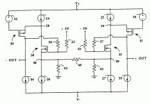
I built some of these (there is more to make up an entire amplifier) to demonstrate simultaneous trimming of Vos and Aol (Aol could be + - or infinite) to debunk the wide open-loop BW folklore. Vos and drift could also be simultaneously nulled.
Can you trim DC as well as ac (THD) with just those two trimmers? Or would you need to trim some others as well to do both?
THx-RNMarsh
Richard, this is the problem with 'simple' solutions. You would fight to get a good compromise between DC offset and AC balance, then would it stay that way indefinitely?
It is better to separate the two functions. I personally chose a servo for DC offset control, and a balance pot for AC. Works just about forever.
It is better to separate the two functions. I personally chose a servo for DC offset control, and a balance pot for AC. Works just about forever.
Can you trim DC as well as ac (THD) with just those two trimmers? Or would you need to trim some others as well to do both?
THx-RNMarsh
Hi Richard,
There are a couple of things at work here, both practically and technically. From a practical point of view, I think adding two trimmers to this circuit is less desirable than matching the parts before installing them. Trimmers add component cost, area and possibly reliability and sound quality issues. They also add labor in setting them, especially if the setting procedure does not converge nearly instantly. Although a PIA, I think hand matching is better in the end.
Then there are the technical issues. DC offset at the output of the amplifier is the least of the problems. It is readily solved by a servo and I believe that is usually the best way to go anyway. However, there are remaining issues of differential offset between like pairs and gate voltage at the chosen operating current. If the P-channel offsets are different, or even go in the opposite direction than the N-channel differential offsets, the pairs will fight at the VAS and the circuit will not perform as well as it can. The trimmers can help this a bit, but I'm not sure they can fix it entirely. I see it as a bandaid at best. Since transconductance in the JFETs depends on operating current, it is not clear to me that after the trimming the transconductances will be the same, as desired. The matching of the devices should not just be minimum offset of a pair, but ideally should be in the same direction for the chosen P-channel pair and N-channel pair that will end up working together.
With regard to transconductance, note also that the gm for P-channel devices is not usually the same as the gm for N-channel devices at a given operating current. In the floating tail arrangement, this means that one pair should be degenerated a bit differently from the other pair, so as to equalize the net transconductances of the pairs. For optimal operation, the P-channel LTP and the N-channel LTP should end up with the same net transconductance. For given JFETs, the relationship between gm and drain current is quite predictable, and remarkably tends to change very little with changes in device-to-device IDSS and VT. This has to do with the BETA parameter in the SPICE model, which tends to be pretty much the same in a given process and geometry despite variations among threshold voltage and IDSS among individual devices.
Finally, the tail bias current in the floating tail arrangement depends on the sum of the absolute values of the threshold voltages of the P and N JFET pairs. If the devices are matched and paired, this sum can also be controlled by putting certain N-channel pairs with certain P-channel pairs, resulting in a more constrained range of tail bias current in the input stage. Depending on the details of the VAS design, the bias current of the input stage can have a large influence over the standing current in the VAS, and this is undesirable.
All of these effects can be easily seen and evaluated with a few simulations.
Cheers,
Bob
We used that common mode feedback style in enhancement/depletion NMOS SRAMs in the 1970s (4kbits, 25nsec), to make the senseamps more immune / less sensitive to enormous step functions in common mode level, caused by the dreaded VccSlew test.... that's a standard CMOS folded cascode with common mode feedback style from the 80's.
JC and Bob --- Thank you for your replies;
I also would rather match devices for ac as well as dc. Then servo as needed for DC/drift. I have been known to trim the harmonic distortion further by slight changes in circuit R's of the compl devices to get a null. Distortion below -120dB can be achieved with low GNFB this way.
THx-RNMarsh
I also would rather match devices for ac as well as dc. Then servo as needed for DC/drift. I have been known to trim the harmonic distortion further by slight changes in circuit R's of the compl devices to get a null. Distortion below -120dB can be achieved with low GNFB this way.
THx-RNMarsh
JC and Bob --- Thank you for your replies;
I also would rather match devices for ac as well as dc. Then servo as needed for DC/drift. I have been known to trim the harmonic distortion further by slight changes in circuit R's of the compl devices to get a null. Distortion below -120dB can be achieved with low GNFB this way.
THx-RNMarsh
This is no feedback and not looking for those kind of numbers. An open-loop diff pair has a compressive odd harmonic dominant behavior that is not trimmable well over the PPM level. Don't need no stink'n servos. Just a little fun in the 8-leg free zone.
- Status
- Not open for further replies.
- Home
- Member Areas
- The Lounge
- John Curl's Blowtorch preamplifier part II