A friend is building the Calvin Buffer. He is concerned that its output DC offset does not settle to zero, until ~ 30 seconds after power-on. He worries that the offset may flow through DC coupled power amps and damage expensive loudspeakers, or just make annoying sounds. So he asked me for a circuit that would mute the Calvin Buffer's output for the first approx. 30 seconds after power on. This board is the result.
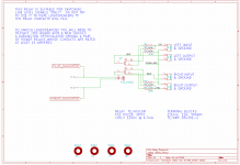
A timing diagram is shown as attachment 1. When AC mains power is switched on, the relay is de-energized and the output remains muted, for 30 seconds. Then the relay is energized and the output becomes unmuted. When AC mains power is switched off, the relay remains energized for 0.8 seconds, then de-energizes and mutes the output.
The power-up delay is adjustable via a 25 turn trimmer potentiometer, from 2 seconds to 40 seconds.
The power-down delay is adjustable via a second 25 turn trimmer pot, from 0.2 seconds to 4 seconds.
The appropriate value of power-down delay is not universally agreed upon. Some people want it to be instantaneous, others want it to be (1 millisecond less than the length of time the amplifiers can run on their internal filter capacitors). So I made it adjustable and the final system integrator can dial in whatever power down delay time he wishes.
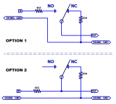
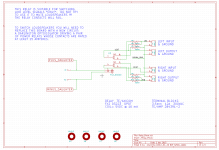
The PCB provides two different ways to mute the output, see attachment 2. I envision R12,R13,R14 as zero ohm resistors ("jumpers"), but the user can stuff any values he wishes. Option 1 puts the relay contacts in the signal path; it mutes the output by disconnecting the output from the input, and then shorting the output to ground (thru R14). In Option 2 the relay contacts are not in the signal path; it mutes the output by shorting the Calvin Buffer itself, to ground (thru R13 and R14).
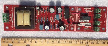
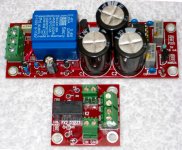
The circuit is built as two independent boards which happen to be fabbed on a single piece of PCB. You can leave it all-in-one, or you can cut the board into two sub-boards, and locate them in different zones of the chassis. Want the relay close to the output jacks, but the transformer far away? No problem. Attachments 3 and 4 show the PCB. There are four guidelines on the text layers, to help you make a straight cut. There is LOTS of clearance here, almost a full centimeter, so precision cutting is not necessary.
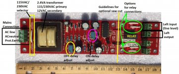
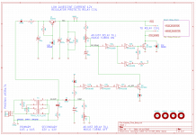
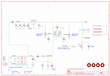
Schematics are shown in attachments 5 and 6. I gave this board its own 2.4VA mains transformer, to sense the mains voltage in the most direct (and IMHO in the safest) manner possible. Zener diode D2 and emitter follower Q1 form a voltage regulator that supplies +12V to the relay coil and to the CMOS digital IC. Big whomping capacitors C2 and C3 store enough energy to keep the coil current flowing for at least 4 seconds after power-off. There is a 2-wire interface between the delay PCB (schematic sheet 1) and the relay PCB (schematic sheet 2). These are the two wires that drive the relay coil. A low power Telecom relay was selected, whose coil resistance is 1800 ohms (6.7 mA at 12V).
The use of a regulated power supply, and a CMOS Schmiitt-Trigger level sensor, makes circuit operation constant and repeatable, despite variations in AC mains voltage level, despite frequency variations (between US and Europe), and despite unit-to-unit variability of relay pull-in voltage.
I constructed the first unit using parts I bought from Digi-Key; a Bill Of Materials including DigiKey part numbers, is included in the attached .zip archive. So are the Gerber files (PCB layout files) that I sent off to a PCB fab in China for board manufacturing. The board worked well, and I have shipped it off to my buddy the Calvin Buffer enthusiast.
I'm placing the design in the public domain; anybody is free to use it however they like, change it however they like, and even sell the darn thing if they can find willing buyers. Have fun with it; make it your own. If you imagine that I might provide unlimited, never-ending technical support on this little gizmo that I built over a weekend and gave away for free -- think again. Plan to call up an engineer friend and buy some beer & pizza.
_
A timing diagram is shown as attachment 1. When AC mains power is switched on, the relay is de-energized and the output remains muted, for 30 seconds. Then the relay is energized and the output becomes unmuted. When AC mains power is switched off, the relay remains energized for 0.8 seconds, then de-energizes and mutes the output.
The power-up delay is adjustable via a 25 turn trimmer potentiometer, from 2 seconds to 40 seconds.
The power-down delay is adjustable via a second 25 turn trimmer pot, from 0.2 seconds to 4 seconds.
The appropriate value of power-down delay is not universally agreed upon. Some people want it to be instantaneous, others want it to be (1 millisecond less than the length of time the amplifiers can run on their internal filter capacitors). So I made it adjustable and the final system integrator can dial in whatever power down delay time he wishes.
The PCB provides two different ways to mute the output, see attachment 2. I envision R12,R13,R14 as zero ohm resistors ("jumpers"), but the user can stuff any values he wishes. Option 1 puts the relay contacts in the signal path; it mutes the output by disconnecting the output from the input, and then shorting the output to ground (thru R14). In Option 2 the relay contacts are not in the signal path; it mutes the output by shorting the Calvin Buffer itself, to ground (thru R13 and R14).
The circuit is built as two independent boards which happen to be fabbed on a single piece of PCB. You can leave it all-in-one, or you can cut the board into two sub-boards, and locate them in different zones of the chassis. Want the relay close to the output jacks, but the transformer far away? No problem. Attachments 3 and 4 show the PCB. There are four guidelines on the text layers, to help you make a straight cut. There is LOTS of clearance here, almost a full centimeter, so precision cutting is not necessary.
Schematics are shown in attachments 5 and 6. I gave this board its own 2.4VA mains transformer, to sense the mains voltage in the most direct (and IMHO in the safest) manner possible. Zener diode D2 and emitter follower Q1 form a voltage regulator that supplies +12V to the relay coil and to the CMOS digital IC. Big whomping capacitors C2 and C3 store enough energy to keep the coil current flowing for at least 4 seconds after power-off. There is a 2-wire interface between the delay PCB (schematic sheet 1) and the relay PCB (schematic sheet 2). These are the two wires that drive the relay coil. A low power Telecom relay was selected, whose coil resistance is 1800 ohms (6.7 mA at 12V).
The use of a regulated power supply, and a CMOS Schmiitt-Trigger level sensor, makes circuit operation constant and repeatable, despite variations in AC mains voltage level, despite frequency variations (between US and Europe), and despite unit-to-unit variability of relay pull-in voltage.
I constructed the first unit using parts I bought from Digi-Key; a Bill Of Materials including DigiKey part numbers, is included in the attached .zip archive. So are the Gerber files (PCB layout files) that I sent off to a PCB fab in China for board manufacturing. The board worked well, and I have shipped it off to my buddy the Calvin Buffer enthusiast.
I'm placing the design in the public domain; anybody is free to use it however they like, change it however they like, and even sell the darn thing if they can find willing buyers. Have fun with it; make it your own. If you imagine that I might provide unlimited, never-ending technical support on this little gizmo that I built over a weekend and gave away for free -- think again. Plan to call up an engineer friend and buy some beer & pizza.
_
Attachments

Last edited:
I made a new PCB revision which shrank the board dimensions. It's now (90 x 31) mm ... 3.5 x 1.2 inches. A few minor circuit details were changed
Photos, schematics, PCB mfg Gerbers, and firmware files are attached.
537 words of program ROM; 58 bytes of RAM; zero bytes of EEPROM
_
- Changed to double insulated miniature transformer by BLOCK
- Changed from analog circuits to 8-pin microcontroller + firmware
- Changed regulated supply from +12V to +5V for the uC
- Changed from discrete voltage regulator to Low Dropout IC Vreg
- Changed relays to one with a +5V coil @ 16mA
Photos, schematics, PCB mfg Gerbers, and firmware files are attached.
537 words of program ROM; 58 bytes of RAM; zero bytes of EEPROM
_
Attachments

Last edited:
A circuit whose output takes 30 secs to settle down probably has too large an output capacitor, or a poorly designed DC servo.
A circuit whose output takes 30 secs to settle down probably has too large an output capacitor, or a poorly designed DC servo.
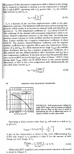
Schematic below. I sort of assumed JFETs operating far away from their zero tempco bias point, might be part of the explanation. Oxner textbook snippet attached.
DIYers being extra extra careful (p a _ _ _ _ i d) might be another part. Dunno.
_
Attachments
For those who inquired:
The firmware in post#2 implements a simple 4-state finite state machine in software. There is only a single input ("AC_present") and it is read via continuous polling. Admittedly an interrupt-based software design would save some amount of power, but (a) the leisurely 500 kHz internal clock is selected, which has already reduced C*V*V*f dynamic power by a factor of 64; (b) even when polling, the microcontroller draws 30X less current than the relay coil, so there's little payoff from reducing uC current further.
The four states of the FSM are named START, TURNON, PLAYMUSIC, and SHUTDOWN; a state transition diagram is attached below.
T1 is the wake-up or power-on delay; the output remains muted (the relay's coil is de-energized) for the first T1 seconds after power-on. Software limits set
T2 is the shut-down or power-off delay; the output remains UNmuted for the first T2 seconds after power-off. This avoids spurious muting when, for example, only a single cycle of the AC mains sinewave (20 msec) is missing. Software limits set
Naturally the FSM diagram below is a simplified representation of the actual software code; it doesn't show A/D conversions, longword arithmetic, and other fine grained details. However the main thrust of the software is fully represented.

OOPS! Image files can't upload to the DIYaudio server! So I'm hosting them on a third-party website. If & when they disappear, it is DIYaudio's fault, not mine!

The firmware in post#2 implements a simple 4-state finite state machine in software. There is only a single input ("AC_present") and it is read via continuous polling. Admittedly an interrupt-based software design would save some amount of power, but (a) the leisurely 500 kHz internal clock is selected, which has already reduced C*V*V*f dynamic power by a factor of 64; (b) even when polling, the microcontroller draws 30X less current than the relay coil, so there's little payoff from reducing uC current further.
The four states of the FSM are named START, TURNON, PLAYMUSIC, and SHUTDOWN; a state transition diagram is attached below.
T1 is the wake-up or power-on delay; the output remains muted (the relay's coil is de-energized) for the first T1 seconds after power-on. Software limits set
- (2 seconds) < T1 < (40 seconds)
T2 is the shut-down or power-off delay; the output remains UNmuted for the first T2 seconds after power-off. This avoids spurious muting when, for example, only a single cycle of the AC mains sinewave (20 msec) is missing. Software limits set
- (200 msec) < T2 < (4 sec)
Naturally the FSM diagram below is a simplified representation of the actual software code; it doesn't show A/D conversions, longword arithmetic, and other fine grained details. However the main thrust of the software is fully represented.
OOPS! Image files can't upload to the DIYaudio server! So I'm hosting them on a third-party website. If & when they disappear, it is DIYaudio's fault, not mine!
Last edited:
Hi,
Why you do not use the zero crossing to turn on the amp? Since your are reading the AC signal with the micro. Depending of the project I used the Zbasic micro or the Basic Micro Nano 8,16 or 28. Both companies have micros compatible with the Arduino UNO. Their basic instructions are better than the Arduino. I am learning now the Arduino because the availability of the cheap boards. I designed my own controller boards.
Why you do not use the zero crossing to turn on the amp? Since your are reading the AC signal with the micro. Depending of the project I used the Zbasic micro or the Basic Micro Nano 8,16 or 28. Both companies have micros compatible with the Arduino UNO. Their basic instructions are better than the Arduino. I am learning now the Arduino because the availability of the cheap boards. I designed my own controller boards.
- It is fitted into a standalone linestage ("the Calvin Buffer") not a power amp
- Its only function is output muting. Turn-on / soft start / inrush limiting is assumed to be handled elsewhere. Or, ignored, since it is fitted into a linestage not a power amp
- Don't forget ELI the ICE man (EE mnemonic for the algebraic sign of phase shift in reactances). Linear power supplies with transformer input, have lowest transformer inrush current when switched on and off at the zero crossing of current, which occurs at the peak of voltage thanks to ELI. Here is Rod Elliott's exposition: (link)
- Status
- Not open for further replies.
- Home
- Amplifiers
- Power Supplies
- Variable-delay output muting PCB for preamps, linestages, et al