hi all
first, i want to say thanks to all this forum that help me to built the F5 2 years ago, i love it 🙂
Now i want to build another F5 to my woofers (100Hz) 🙂
i have ready to use -+30vdc power supply that i build for class AB.
There is simple way to down to 25v ? Diode?
i have 25W 100ohm resistor if its help 🙂
Thanks
the last time i connected 30vdc to my F5, the 2sk blow.
Last edited:
You can build the F5 with +-30VDC. You will have to use bigger heatsinks to dissipate the heat or bias at a lower value. You can also try the F5turbo or F5cascode, with extra output transistors. It might help to control the woofers as having more output devices should increase control over the speakers.
what about the jfet?
not need to change any resistor in the jfet stage?
ok i try with the 30vdc
i have 70cm heatsinks 🙂 no problem
thanks
not need to change any resistor in the jfet stage?
ok i try with the 30vdc
i have 70cm heatsinks 🙂 no problem
thanks
This is what Nelson says about the JFETs running at 32V:
So you would expect them to survive the 32V, maybe the Idss is high? Do you know what Idss they are?
"The more technically astute DIYer may note that the input Jfets are now
being exposed to greater voltage and dissipation, and this might be a
concern. With respect to voltage, the operating point of these devices is
around 30 volts, 5 volts over their rating. In actual testing these devices
break down around 43 volts, and I depend on Toshiba's famed conservatism
to carry the day. If you don't want to trust Toshiba as much as I do, then you
can cascode these devices, which is covered here later.
The average dissipation of the Jfets with a 32V supply will be about 28 volts
times the operating current. A 2SK170 or 2SJ74 with a 10 mA Idss will
operate at about 8 mA in this circuit, which gives a dissipation of about 220
mW. A quick calculation shows that its maximum junction temperature at 220
mW is reached with an ambient temperature of about 70 deg C. A wise DIYer
will either select a Jfet with a lesser Idss (say 8 mA) and/or see to it that the
Jfets gets some cool air or a little heat sink. Or you can cascode them."being exposed to greater voltage and dissipation, and this might be a
concern. With respect to voltage, the operating point of these devices is
around 30 volts, 5 volts over their rating. In actual testing these devices
break down around 43 volts, and I depend on Toshiba's famed conservatism
to carry the day. If you don't want to trust Toshiba as much as I do, then you
can cascode these devices, which is covered here later.
The average dissipation of the Jfets with a 32V supply will be about 28 volts
times the operating current. A 2SK170 or 2SJ74 with a 10 mA Idss will
operate at about 8 mA in this circuit, which gives a dissipation of about 220
mW. A quick calculation shows that its maximum junction temperature at 220
mW is reached with an ambient temperature of about 70 deg C. A wise DIYer
will either select a Jfet with a lesser Idss (say 8 mA) and/or see to it that the
So you would expect them to survive the 32V, maybe the Idss is high? Do you know what Idss they are?
thanks
i have 2sk246 4ma idss, i can cascade them for start.
i have 2sk117 2ma idss too, and 2sk170 20pcs,
try to find 8ma and play with it.
thanks 🙂
i have 2sk246 4ma idss, i can cascade them for start.
i have 2sk117 2ma idss too, and 2sk170 20pcs,
try to find 8ma and play with it.
thanks 🙂
Higher Voltage F5
The F5 needs sufficient current capability in the input stage to drive the loads.
I suggest you don't go below a BL grade lower limit of 6mA Idss.
The better solution is to use the cascode as described in the F5t.
You can build cascode as a hardwired pair of jFETs with just 3 legs that plug straight into the 3 pads/holes in a standard F5 PCB.
yes, 2SJ74, but i buy theme chip so maybe its fake, its only one channel so its no problem to buy.
in the past i use 3 parallel 2sk246 for testing, try to find 6-8 ma from my stock
in the past i use 3 parallel 2sk246 for testing, try to find 6-8 ma from my stock
Last edited:
The F5 needs sufficient current capability in the input stage to drive the loads.
I suggest you don't go below a BL grade lower limit of 6mA Idss.
The better solution is to use the cascode as described in the F5t.
You can build cascode as a hardwired pair of jFETs with just 3 legs that plug straight into the 3 pads/holes in a standard F5 PCB.
Doesn't the cascode require a few resistors as well? Can you direct to a diagram of this? I have hesitated to cascode on boards not designed for it. Your solution sounds like a nice neat package using the existing 3 jfet holes.
Thanks,
Russellc
Select a high Idss, low gm, jFET for the cascode device.
Select a much lower Idss, high gm device for the amplifier device.
Connect cascode Source to amp Drain
Connect cascode Gate to amp Source
You are left with the Cascode Drain that enters the original D pad,
The amp Gate goes to the original G pad.
The junction of amp Source and cascode Gate go to the original S pad.
If you select an appropriate cascode device it will give a Vds(amp) >> Vp of amp device.
It could be >3Vds
Now the dissipation in the amp is 10mA*0.8 * 3Vds ~24mW
The cascode dissipation is 10mA*0.8 * Vds. where Vds is ~ 3Volts less than if a single jFET were used. say the supply is 32V then Vds ~ 28V New Vds is ~28-3 = 25V
and dissipation is ~8mA * 25V ~ 200mW
The amp device runs near cold and the cascode becomes the highly stressed device.
Doesn't the cascode require a few resistors as well? Can you direct to a diagram of this? I have hesitated to cascode on boards not designed for it. Your solution sounds like a nice neat package using the existing 3 jfet holes.
Thanks,
Russellc
read F5T article
read F5T article
That is what my comment was based on. When I bought into Buzzborbs Turbo F5 group buy, (which I ended up selling) the bag of parts for adding the cascode, and spots on the circuit board were several. Andrews method sounds compact and easy to graft on, but I dont have any low idss devices for the amp, all mine are a little on the high (8-9) side.
I will re read the T F-5 article again.
Russellc
It's a waste of energy to blow class A heat on woofers. Put the extra heat into your existing F5 for the top end.
But you can still build another F5, but just don't bias it so hard.
But you can still build another F5, but just don't bias it so hard.
Totally agree. Run with the higher rails and less output bias, and let the F5 spend more time in class A/B, provided your input jfets are OK.It's a waste of energy to blow class A heat on woofers. Put the extra heat into your existing F5 for the top end.
But you can still build another F5, but just don't bias it so hard.
Buy some TO-92 heatsinks that just slip on.
Put a little thermal grease on the Jfet and it will help control the package temperature.
Put a little thermal grease on the Jfet and it will help control the package temperature.
It's a waste of energy to blow class A heat on woofers. Put the extra heat into your existing F5 for the top end.
But you can still build another F5, but just don't bias it so hard.
Nice tip Andersonix
i have F5 for my FR speaker, its run hot bias 1.5A
My heatsink warm to 40 deg, 70*30cm heatsink ! So i have place for another F5 i think.
About the woofer bias, i start with 0.5A.
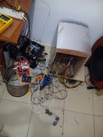
OK, I build the first stage yesterday:
Found 8.5mA 2sk170/74, Recommendations for 30vdc.
No ZTX, no NTC for now, very simple 🙂
33Vdc PS
No IRF connected
Results:
Nice and clean sin wave
The 2sk/j is worm but not hot (touch with hands)
The gain is ~30
Today i try connected the IRF
Thanks thanks, my 15" OB woofer can't wait 🙂
Attachments
Nice tip Andersonix
i have F5 for my FR speaker, its run hot bias 1.5A
My heatsink warm to 40 deg, 70*30cm heatsink ! So i have place for another F5 i think.
About the woofer bias, i start with 0.5A.
OK, I build the first stage yesterday:
Found 8.5mA 2sk170/74, Recommendations for 30vdc.
No ZTX, no NTC for now, very simple 🙂
33Vdc PS
No IRF connected
Results:
Nice and clean sin wave
The 2sk/j is worm but not hot (touch with hands)
The gain is ~30
Today i try connected the IRF
Thanks thanks, my 15" OB woofer can't wait 🙂
I like the pic. That's real diy!
Last edited:
- Status
- Not open for further replies.
- Home
- Amplifiers
- Pass Labs
- F5 power supply to high, solution?