Hi guys (and gals!)
Most of you probably think that any half-decent power converter has to be based on the latest chip from TI or Linear.
50 years ago, things were very different: self-oscillating converters ruled, asymetrical for low power, push-pull for P>~5W.
Those topologies have now been rendered completely obsolete....
Really?
I have played with the basic PP topology, standard TTH components and materials, but I also used a bit of lateral thinking.
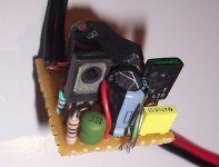
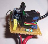
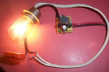
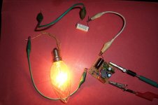
Here is the result:

Litterally, a thumb-sized converter. The interesting thing is that this tiny converter is capable of transferring a power in excess of 40W, without any heatsink.

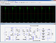
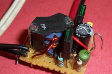
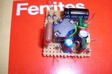
The circuit is very similar to what could be found 40 to 60 years ago:

The main differences are in the base drive section: only one feedback winding is used, and the base circuit also includes a series resonant circuit.
This tank has the effect of stabilizing the frequency at ~60KHz, but it also takes care of the progressive desaturation of the transistors.
This allows the use of slow transistors (Ft=3MHz) without efficiency penalty (the transistors actually used are BD439's, ideally they should be BD435 or 7).
Another trick, much less obvious, is the presence of zeners diodes in anti-parallel with the base.
Why zener diodes?
Diodes are required to ensure the continuity of the base current path, but they never see more than ~1V reverse.
Zener (avalanche in fact) diodes have the interesting property of having a storage time ~proportional to their breakdown. In this case, with 30V, it is approximately 300ns (it also heavily depends on the series). I handpicked the ones that had the right value for me.
When the converter is switching, they keep the inactive transistor OFF for a bit longer, allowing a natural (lossless) switching by the transformer's inductance.
Thanks to these tricks, the switching losses are practically eliminated, and since the BD43x have a very healthy and energetic conduction, the overall losses are also very low.
This converter can be made to tolerate an incandescent lamp load, and the secondary can be highly isolated: in this example, the transformer uses a split-bobbin:


These features make it ideal as a heater driver (it could also be used for HV generation though).
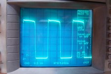
Here is the waveform on one of the collectors:

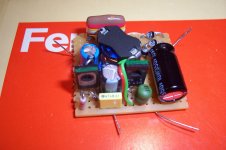
The tank components:

To be continued....
PS
As the pics don't seem to appear, I also attach them:
Most of you probably think that any half-decent power converter has to be based on the latest chip from TI or Linear.
50 years ago, things were very different: self-oscillating converters ruled, asymetrical for low power, push-pull for P>~5W.
Those topologies have now been rendered completely obsolete....
Really?
I have played with the basic PP topology, standard TTH components and materials, but I also used a bit of lateral thinking.
Here is the result:
Litterally, a thumb-sized converter. The interesting thing is that this tiny converter is capable of transferring a power in excess of 40W, without any heatsink.
The circuit is very similar to what could be found 40 to 60 years ago:
The main differences are in the base drive section: only one feedback winding is used, and the base circuit also includes a series resonant circuit.
This tank has the effect of stabilizing the frequency at ~60KHz, but it also takes care of the progressive desaturation of the transistors.
This allows the use of slow transistors (Ft=3MHz) without efficiency penalty (the transistors actually used are BD439's, ideally they should be BD435 or 7).
Another trick, much less obvious, is the presence of zeners diodes in anti-parallel with the base.
Why zener diodes?
Diodes are required to ensure the continuity of the base current path, but they never see more than ~1V reverse.
Zener (avalanche in fact) diodes have the interesting property of having a storage time ~proportional to their breakdown. In this case, with 30V, it is approximately 300ns (it also heavily depends on the series). I handpicked the ones that had the right value for me.
When the converter is switching, they keep the inactive transistor OFF for a bit longer, allowing a natural (lossless) switching by the transformer's inductance.
Thanks to these tricks, the switching losses are practically eliminated, and since the BD43x have a very healthy and energetic conduction, the overall losses are also very low.
This converter can be made to tolerate an incandescent lamp load, and the secondary can be highly isolated: in this example, the transformer uses a split-bobbin:
These features make it ideal as a heater driver (it could also be used for HV generation though).
Here is the waveform on one of the collectors:
The tank components:
To be continued....
PS
As the pics don't seem to appear, I also attach them:
Attachments

Last edited:
I did my university thesis on switch mode power amplification (PWM).
The earliest large scale production I found in my literature search was a 48VDC to 24VDC converter for phone companies made by Philips from about 1962, using the ASZ16-series gnermanium power transistors. It had a fully regulated output, stable on all loads reactive or resistive from zero to full load (several amps) and had short circuit protection and very low EMI.
The earliest PWM audio power amplifier in large scale production was the 1964-odd Sinclair X10, rapidly replaced by the X20 in 1965. These were very very crude in circuit design and execution (Clive Sinclair was notorious for buying batches of factory reject transistors via the "back door"). On instrument test they appeared to be absolutely disgusting. But I have kept an X20 ever since, as it actually sounds quite good. Not high quality, but MUCH better than the test gear indicates. Much like a tube SE amp in its' sound. I demonstrate it sometimes to show people that THD testing is NOT a measure of amplifier objectionableness.
When I was at school (late 1950's), and mad keen on building stereo amplifiers and other electronic devices, a large fraction of men in my town worked in a nearby huge railroad maintenance depot. Train carriages had lighting powered by an on-board generator turned by one pair of wheels. This charged a 24 V lead acid battery. The flourescent lights used in the (then) late model carriages used a 2-transistor invertor based on fast germanium power transistors rated at 80 volts CE.
Apparently the switching transients in these lighting invertors were not well controlled and the transistors often failed. They didn't fail completely - they developed high leakage that rapidly increased when the collector voltage went over about 45 to 55 volts.
Railway guys used to give us the failed power transistors. Used in a stereo amplifier with a DC supply less than 45 V they worked just fine. But their bandwidth was vastly superior to the consumer grade power transistors then used in audio. So I got to make what was for the time, very very good stereo amps, for very little cost. With the usual 2N301 or AD149 power transistors then, their bandwidth was as low as 8 kHz, so making an amp that was stable, and had well controlled crossover distortion was rather difficult. But with those reject railway transistors, no problem at all.
12V to 240 VAC invertors for car and caravan (=trailer home for US folk) based on simple germanium transistor circuits were once common, from about 1960 onward. As were simple one-transitor invertors for camera flash guns.
Last edited:
More ingenious work, Elvee, always enjoyable to read.
The circuit architecture looks like a basic version of the Royer converter (sans PWM input) that was still used a great deal in computer backlight inverters for CCFL lamps, until LED lighting supervened in that application.
My own design for a CCFL lamp driver (for the HUSKY fex21 series) used the Zetex FZT853 (=ZTX853 for through hole) for the switching transistor. This transistor had astonishingly low Vce(Sat) for the day (0.02V @0.5A easily achieved in a typical sample), and made quite a difference to battery life. I bet it would still be hard to beat, 17 years on.
Is L6 a representation of leakage inductance?
Thanks for sharing!
Philips telco converters were very well designed: they used current feedback, and the control was achieved through magnetic means. Some were based on mag amps, others used a form of magnetic pulse width modulation.
Performances were excellent, but they are in a different league compared to this series.
The number of custom magnetic parts was rather large. Here, there is a single coupled element that is pretty straightforward to make.
There is no control, protection, or advanced features: it is the electronic equivalent of a dumb transformer.
For applications like a heater, it is normally sufficient. It is always possible to include a pre- or post-regulator if a great accuracy is required.
The design of the transformer is rather straightforward: the most important is to ensure that the volt*second at the primary does not exceed the core capacity.
This requires a number of turns n = Vs/(4*B*F*Ae)
Vs: V supply (Volt)
B: peak tolerable induction in the core (Tesla)
F: Nominal frequency (Hz)
Ae: Effective core area (m²)
With a 12V supply, 60KHz switching frequency and the RM6 core used as example, a safe induction value is B=250mT for example for the N41 material (I know: my prototype uses N47, but I could have sworn it was N41, until of course I used a magnifying lens...)
Thus, n= 12/(4*0.25*60e3*36.6e-6) =5.46 => 5.5 turns for each half primary.
The copper section depends on the current. For small transformers, highish current densities like 10A/mm² are tolerable.
The feedback winding must deliver approximately 3~4V peak for a reliable operation.
The secondary needs a small supplement of turns to compensate for the internal impedance of the converter (mainly caused by the leakage inductance).
When the coupling is poor like here, the leakage can be compensated by a series capacitor. It could also be left uncompensated and serve as a ballast.
If the converter has to frequently work under low or no load, it is preferable to include D7 and D8: they provide a deterministic path for the recuperation of the energy stored in the transformer.
Otherwise, recuperation has to rely on the reverse beta of the transistors, which is less effective.
R2 and R3 allow the startup, the value of 4.7K is a tradeoff: it allows to start on moderately difficult loads, without too much impacting the low current efficiency.
It would be possible to use much higher permanent values, like 100K, and connect lower ones temporarily during the startup: 470 ohm for example.
The output could be used directly in AC, or rectified (and maybe regulated).
On my prototype, at Pout=40W with a schottky rectifier bridge, the overall efficiency is 86%. Most of the losses come from the bridge (~30%), 25% for the transformer (this high value is mainly caused by the unsuitable N47 material), 20% for the transistors and 15% in the base drive.
It would of course be possible to use a center-tapped secondary, or multiple isolated secondaries.
To be continued.....
Yes, the Zetex (now Diodes Inc) transistors would be more suitable than the BD43x: they have comparable saturation characteristics but a higher Hfe and they are faster tooMy own design for a CCFL lamp driver (for the HUSKY fex21 series) used the Zetex FZT853 (=ZTX853 for through hole) for the switching transistor. This transistor had astonishingly low Vce(Sat) for the day (0.02V @0.5A easily achieved in a typical sample), and made quite a difference to battery life. I bet it would still be hard to beat, 17 years on.
Yes, I chose to show it explicitly because this winding is much less coupled than the othersIs L6 a representation of leakage inductance?
Philips telco converters were very well designed: The number of custom magnetic parts was rather large.
As I recall, there was a single ferrite core transformer, based on 4 large rectangular U-cores. There were custom in the sense that the design was specific to the inverter. They would hardly be anything else. The cores were a then rare type but not custom. Similar to Siemens U93 series.
There were several TO1 germanium transistors effecting control.
Last edited:
A few additional details:
Transformer:
The dimensioning I outlined above ensures the core never saturates, which is essential.
However, with small, low voltage converters, the number of turns obtained that way may result in a very low magnetizing inductance. This means that the magnetizing current can be of the same order as the active current, which is not desirable since it uselessly generates heat in the primaries.
If there is still room in the winding window, it can be advantageous to fill it up more completely.
That's what I should have done: I still had room for 1 or 2 turns, and it would have somewhat improved the lowish 50µH primary inductance.
I didn't do it, because at that time I was still convinced I was using material N41, whose permeability is more than twice that of the N47.
The ferrite should preferably be a power one, like N41, 3C81, etc, but not necessarily: in fact, any MnZN will do, provided the induction is adapted.
I made my first tests with common mode chokes, as they come pre-wound with two symmetrical windings, and it worked perfectly. Of course, the induction was very low because the number of turns was rather large.
For the primaries, bifilar winding should be used as it reduces unwanted inductive spikes.
For these small transformers, very high current densities are acceptable: 10A/mm² for example.
Base drive:
The feedback winding should be dimensioned to provide approximately 4V^ with the nominal supply voltage (not critical).
The RLC network can be adapted if the power is smaller than 40W: R and L can be increased and C decreased in the same proportion, this will not change the operating frequency, just the level of base drive.
The base diodes can be suitable zeners, but be aware that the recovery time is not specified for these components and there might be large variations.
More deterministic options include band switching diodes for TV tuners and non-gold-bonded general purpose signal diodes like the OA200 or the 1N646.
1N400x diodes have a trr of a few µs, leading to excessive dead-times.
Secondary winding
Even when the circuit does not require it, it is preferable to also wind it in bifilar: this will reduce common mode perturbations to insignificant levels, and provide a "cold point" where to connect a small "Y" capacitor.
If it has to be physically separated from the rest of the windings, it can be tuned with a series capacitor, as in my example. This is made possible thanks to the good stability of the frequency.
Here is an example of "kickstarter" circuit for difficult loads.
With the values shown, the startup period is ~1 second, and proportional to C3.
R8 can be added to help the restarting in case the converter stops for some reason (momentary surge in the load current for example).
Without it, the converter is inherently protected against shorts: it will simply stop, and not restart by itself
Attachments

Hadn't seen the case with resonant commutation, interesting.
There might be additional benefit from using a saturable reactor there, assuming you can design its value and saturation point so its current peaks just as switching occurs, given the base drive amplitude.
The usual case (no series supply inductor) has shorting mode commutation, where load inductance causes increasing collector current, while capacitive drive coupling causes decreasing base current; drive falls below hFE(sat), collector voltage rises, and afterwards, the transistor switches off and collector current falls. This can be enhanced with a saturating transformer (so that the collector voltage is made to rise more sharply), or by using emitter current sense transistors (like here http://seventransistorlabs.com/Images/Deadbug_Sch.png ).
The "Royer" oscillator (actually due to Baxandall, yes the one and only) uses a series inductance in the supply, so that when shorting mode commutation occurs, it does so at zero voltage. Here, the collector load is resonant, so this occurs naturally and periodically. (The reactive current from the supply inductor feeds the circuit, but since it sees twice the frequency, it has a lopsided effect, changing the waveform's odd harmonics, so is usually made much larger than necessary.)
You could also use a series supply inductor with the square wave (nonresonant, hFE or saturation commutated) circuit, but its flyback energy needs to be handled on every half cycle; an RC damper or RCD clamp might be used.
Tim
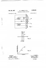
Royer's Patent (For Westinghouse, April 1954) does not demand a mandatory series supply inductor (see picture from the patent). Not in the basic version, anyway. Adding the inductor improves the circuit in the way you describe, to reduce stress on the switching elements.
But for flourescent lamp converters, using this method yes, the collector load must be resonant, not least so that a practical optimisation between transformer design and lamp uniformity & losses can be achieved. Tuning can be achieved with a collector-to-collector capacitor.
The series supply inductor used for this application allows the circuit to be driven from PWM circuits, to give a range of permissible supply voltages, and control power level without losing efficiency.
Was Baxendall really working on these oscillators before 1954?
Attachments
Last edited:
It could be, but it would be delicate: the frequency would become dependent on the supply voltage, and in my experience when you use saturable inductors in circuits involving positive feedback, the results can be completely unexpected and counter-intuitive: the circuit could lock itself into a completely spurious mode or become (literally) chaotic.Hadn't seen the case with resonant commutation, interesting.
There might be additional benefit from using a saturable reactor there, assuming you can design its value and saturation point so its current peaks just as switching occurs, given the base drive amplitude.
Yes, that is how most converters traditionally work, but unlike this one, it makes their frequency sensitive to the load, power supply, or both.The usual case (no series supply inductor) has shorting mode commutation, where load inductance causes increasing collector current, while capacitive drive coupling causes decreasing base current; drive falls below hFE(sat), collector voltage rises, and afterwards, the transistor switches off and collector current falls. This can be enhanced with a saturating transformer (so that the collector voltage is made to rise more sharply), or by using emitter current sense transistors (like here http://seventransistorlabs.com/Images/Deadbug_Sch.png ).
I am afraid that by just using the Royer (or Baxandall) inductor without the rest of the kit, you will end up with disadvantages mainly, unless you implement complicated recuperation schemesYou could also use a series supply inductor with the square wave (nonresonant, hFE or saturation commutated) circuit, but its flyback energy needs to be handled on every half cycle; an RC damper or RCD clamp might be used.
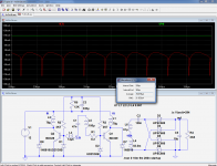
An advantage of the purely square wave operation is that the stress on the output filter cap is minimal: there are no charging peaks to speak of, and this leads to a very small rms current.
In the example below, the rms current through the cap is just 22mA for a 120mA output.
I have tested this idea for higher voltages: in this example, the target voltage is ~300VDC output.
The circuit remains mostly identical, except for some minor adaptations (and a different secondary, obviously).
This time, I used the proper ferrite grade (N41), and 6 turns for each primary.
The windings are superposed instead of split: this results in a smaller leakage inductance, which is not necessarily an advantage: I noticed that the startup is significantly less energetic than for the previous version: I had initially used 2 turns for the reaction winding, but I had to increase it to 2.5t, and reduce R1 to 8.2Ω.
Even then, the converter doesn't start on a load lower than 2.3KΩ or a filter cap larger than ~25µF. Once started, it happily accepts easily 50W (and probably more, but I didn't dare go higher), but that remains relatively weak compared to the other one.
A word of caution for those trying to reproduce my results: I have used BD439's from Telefunken, and these are truly excellent: fast, low Vcesat, high Hfe at high current....
It is probable that even a BD435 from a contemporary manufacturer like Fairchild or ONsemi couldn't reach that level of performance
Attachments
Some more facts about this converter:
-The minimal supply voltage for a reliable startup is just under 0.6V (no load, but with 10µ output cap).
-With 12V input and no load at all, the output voltage creeps asymptotically to ~350V (very slowly).
With a 1 Megohm bleeder resistor, the voltage stays stable at 330V
-The minimal supply voltage for a reliable startup is just under 0.6V (no load, but with 10µ output cap).
-With 12V input and no load at all, the output voltage creeps asymptotically to ~350V (very slowly).
With a 1 Megohm bleeder resistor, the voltage stays stable at 330V
- Status
- Not open for further replies.
- Home
- Amplifiers
- Tubes / Valves
- A bit of fun with archaic converters