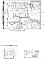
The Left volume control pot assembly (JP105-1) is located between the output of the first opamp in IC101 and the input of the second. Likewise, the Right channel volume pot assy. (JP105-2) is between output of the first in IC102 and the input of the second.
To express that another way, the volume pots are in series with signal from flowing from R113 to R127 (L) and R124 to R128 (R).
i.e. It's a traditional buffered volume control, as you call it. Note that the bridging switch removes the normal input signal to the 2nd opamp in the right channel when in bridged mode and drives its inverting input from the left channel instead.
Last edited:
Thank you for putting effort into that answer, i appreciate it
If that is the case, would it be possible to bypass the volume PCB by jumpering 1 and 3 (JP105-1, edge of input board on the diagram) and 3 and 1 (JP105-2, edge again)?
If that is the case, would it be possible to bypass the volume PCB by jumpering 1 and 3 (JP105-1, edge of input board on the diagram) and 3 and 1 (JP105-2, edge again)?
You could do that, but the volume levels will be as if set at maximum volume and probably a bit noisy when only fed with low to moderate signal levels. To give more equivalence to the existing circuit, fit resistors of value equal to the volume pots, in parallel with R115, R116. I can't tell what value they should be without looking at the pots. You could also calculate a single resistor to replace both if you wish. The isolating caps, C901,902 should also be refitted by connecting the 2 opamp stages with them as they do now, to avoid DC and offset problems.
very special and not usual at most other power amp models are two different inputs - one with the subsonic (high pass) filter (12db/oct).
Actually the "LAB" input is the normal input and the "NORMAL" input is those with subsonic filter in the signal path.
I do not recommend to use this amplifier in the bridge mode, because the sound quality suffers in most cases (maybe except in cases, where the lowest speaker impedance don't goes below 8 ohms).
Last edited:
The connections ar numbered somewhat unclear.Hi guys
I'm having trouble interpreting -- is the input volume PCB controlling the gain of the opamps or is it actually in the signal path like a traditional volume control?
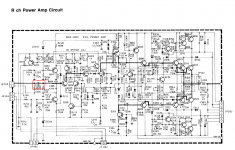
Schematic diagram is attached
THANK YOUUU
Mona
Attachments

You could do that, but the volume levels will be as if set at maximum volume and probably a bit noisy when only fed with low to moderate signal levels. To give more equivalence to the existing circuit, fit resistors of value equal to the volume pots, in parallel with R115, R116. I can't tell what value they should be without looking at the pots. You could also calculate a single resistor to replace both if you wish. The isolating caps, C901,902 should also be refitted by connecting the 2 opamp stages with them as they do now, to avoid DC and offset problems.
youve been very helpful, thank you. there are caps at the input, and then again on the input to the main power amp boards, so could C901 and C902 be eliminated in the new volume control-less circuit?
Yes and no, one C stays.there are caps at the input, and then again on the input to the main power amp boards, so could C901 and C902 be eliminated in the new volume control-less circuit?
Mona
Attachments
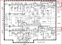
Yes and no, one C stays.
Mona
so basically, one cap has to stay inbetween the op-amps?
because that's what I would like to bypass most of all.
The C120 in the other channel is missing on board in the upper one.They put it on the vol.***..Without it the capacitor has to be put on the board.It prevents the offset voltage of the pre to enter the poweramp.Could give DC on the output (speakers).
Mona
Mona
- Status
- Not open for further replies.
- Home
- Amplifiers
- Solid State
- Schematic help! Take a look at this NAD 2600A diagram