Yes - that's a significant step in the right direction.
Next refinement would be to give the input (to the volume control and source) and output 0V returns each a separate track back to the same common node between power and signal grounds. The reason for this is that input/output grounds are normally carrying common-mode noise and its best not to couple that noise into signal nodes via common impedance coupling.
Next refinement would be to give the input (to the volume control and source) and output 0V returns each a separate track back to the same common node between power and signal grounds. The reason for this is that input/output grounds are normally carrying common-mode noise and its best not to couple that noise into signal nodes via common impedance coupling.
It's not just about how small, it's about how small 'stray' inductance and capacitance.
SMT caps have no leads, hence no lead inductance. That doesn't mean there's NO inductance, but it's greatly reduced, and hence the effect of the caps is greatly enhanced. Reduced stray capacitance reduces the likelihood of unforseen feedback.
Look at this buffer
You can see details of the grounding, power supply, input and output nets highlighted in this thread: http://www.diyaudio.com/forums/solid-state/267136-32-opamps-50mm-square-buffer.html
When I say 'line astern' I mean yours are in 'line abreast'. Didn't you ever watch a Navy movie?
Floodfilling means 'filling an area with copper automatically avoiding explicit tracks and joining it to a net (typically ground)'
When I say running primary ground under the opamps, I mean that the cutaway right under the opamp is probably not useful. Some cutaway under the pins and feedback components yes, but you are denying yourself a useful line-of-sight path for ground organised on a single track running from power inlet to output connector to power amp to gain amp to input amp to input connector, with the feedback ground returns distributed more or less along the line in order of current magnitude.
Electrolytics. Big, high capacity, smoothing, square capacitor jobbies.
SMT caps have no leads, hence no lead inductance. That doesn't mean there's NO inductance, but it's greatly reduced, and hence the effect of the caps is greatly enhanced. Reduced stray capacitance reduces the likelihood of unforseen feedback.
Look at this buffer
An externally hosted image should be here but it was not working when we last tested it.
You can see details of the grounding, power supply, input and output nets highlighted in this thread: http://www.diyaudio.com/forums/solid-state/267136-32-opamps-50mm-square-buffer.html
When I say 'line astern' I mean yours are in 'line abreast'. Didn't you ever watch a Navy movie?
Floodfilling means 'filling an area with copper automatically avoiding explicit tracks and joining it to a net (typically ground)'
When I say running primary ground under the opamps, I mean that the cutaway right under the opamp is probably not useful. Some cutaway under the pins and feedback components yes, but you are denying yourself a useful line-of-sight path for ground organised on a single track running from power inlet to output connector to power amp to gain amp to input amp to input connector, with the feedback ground returns distributed more or less along the line in order of current magnitude.
Electrolytics. Big, high capacity, smoothing, square capacitor jobbies.
Yes that would have the same effect. I would still move the via from out of the pad and have a short stub route to it.
I wonder weather you do need to remove the ground plane under the AD's for the frequencies you using it at.
I wonder weather you do need to remove the ground plane under the AD's for the frequencies you using it at.
Yes that would have the same effect. I would still move the via from out of the pad and have a short stub route to it.
I wonder weather you do need to remove the ground plane under the AD's for the frequencies you using it at.
Not sure what a stub route is.
If you can modify one of the photos I've posted and add these stub routes, perhaps I can understand what you're talking about.
Rayma suggested the ground plane on the bottom. So now I don't need a ground plane at all?😕
Rayma suggested the ground plane on the bottom. So now I don't need a ground plane at all?😕
You'll likely need a ground plane with such high speed devices.
It's not just about how small, it's about how small 'stray' inductance and capacitance.
SMT caps have no leads, hence no lead inductance. That doesn't mean there's NO inductance, but it's greatly reduced, and hence the effect of the caps is greatly enhanced. Reduced stray capacitance reduces the likelihood of unforseen feedback.
Look at this buffer
An externally hosted image should be here but it was not working when we last tested it.
You can see details of the grounding, power supply, input and output nets highlighted in this thread: http://www.diyaudio.com/forums/solid-state/267136-32-opamps-50mm-square-buffer.html
When I say 'line astern' I mean yours are in 'line abreast'. Didn't you ever watch a Navy movie?
Floodfilling means 'filling an area with copper automatically avoiding explicit tracks and joining it to a net (typically ground)'
When I say running primary ground under the opamps, I mean that the cutaway right under the opamp is probably not useful. Some cutaway under the pins and feedback components yes, but you are denying yourself a useful line-of-sight path for ground organised on a single track running from power inlet to output connector to power amp to gain amp to input amp to input connector, with the feedback ground returns distributed more or less along the line in order of current magnitude.
Electrolytics. Big, high capacity, smoothing, square capacitor jobbies.
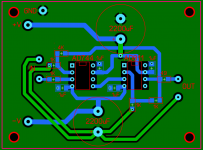
Thank you for the example Counter, but quite honestly I can't make heads or tails out of that board. I don't think I can see the forest for all the trees as they say.🙂
Looks like you crammed a LOT of components in a small space, which is very impressive.
Can you please post a photo of a buffer with only a couple of ICs instead of 32?
Thanks...
Yes - that's a significant step in the right direction.
Next refinement would be to give the input (to the volume control and source) and output 0V returns each a separate track back to the same common node between power and signal grounds. The reason for this is that input/output grounds are normally carrying common-mode noise and its best not to couple that noise into signal nodes via common impedance coupling.
I dont understand.
Good layout starts with good component layout.
What are our intentions? To keep the inputs away from the outputs and to keep the PSU rails away from both, with the minor exception of the load ground return.
To provide adequate decoupling at the device power pins.
To arrange in general that the power supply rails and ground returns connect the PSU ground and rail connections first to the noisiest parts of the circuit (most power-consuming) and thence progressively to less noisy parts of the circuit, in the case of the ground rail the input ground will generally be at the quietest point, with the feedback returns somewhere in the middle.
These being class B amplifiers the power rails should be run in as close proximity to each other as possible.
Here's a dual-channel Jung Multiloop with AD8397 & LME49725 with OPA2277 DC servo. The outputs have provision for a handwound inductor and parallel resistor, but no Zobel. I cut it out of another design I abandoned because the AD8397 is known to pop on short-circuit, and the protection circuit was a pain.
You will see that U2, the AD8397 has a large via beneath it, connecting copper pours on both top and bottom. This is to permit the central grounding pad to be soldered, for heatsinking purposes. I would give this a bit more attention in a later version. You can still see the areas near the AD8397 which have had the pours excluded, however.
Many designs operate under constraints with regard to ergonomics. We want the input, volume control and output in a line. We want to bring power to the rear of the board (maybe not). Miniature jacks do nothing for crosstalk. We want a single board without flying leads. We want to manufacture prototypes on the CNC router. This may lead to some compromises. We need to expect a respin of the layout if test shows that it is not up to scratch and not be paralysed at the prospect. This is how we avoid pointless recriminations, make progress and learn.
An externally hosted image should be here but it was not working when we last tested it.
An externally hosted image should be here but it was not working when we last tested it.
Crude 3D visualizations:
An externally hosted image should be here but it was not working when we last tested it.
An externally hosted image should be here but it was not working when we last tested it.
Thank you for posting the other example. It's a lot easier to make out than that 32 op-amp monster.🙂
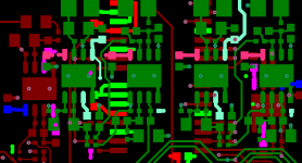
For me, all the pinks, reds and blues are confusing me.
I just can't tell what traces are on which layer.
If you could please post photos of each individual layer, perhaps I can understand more about what should go where.
If not, then I understand as you've been more than patient with me.
For me, all the pinks, reds and blues are confusing me.
I just can't tell what traces are on which layer.
If you could please post photos of each individual layer, perhaps I can understand more about what should go where.
If not, then I understand as you've been more than patient with me.
I dont understand.
If you're desirous of understanding please highlight which part you weren't able to grasp. I'll then do my best to elucidate. In the absence of questions I'll just assume you're quite content in your lack of understanding,
Next refinement would be to give the input (to the volume control and source) and output 0V returns each a separate track back to the same common node between power and signal grounds.
That's what I don't understand. I thought my statement was pretty self-explanatory, but apparently it wasn't.
With all the screen snapshot software available, why not just take the image of the last board I posted and draw the appropriate trace(s) with say Microsoft Paint, and then attach the revised board image to your post?
If not, maybe you can explain where the traces should go.
Thanks...
OK, I have dimmed the planes.
Components with RED pads and CYAN silkscreen are closest to you, normally COMPONENT side, components with BLUE pads and MAGENTA silkscreen are on the other side of the PCB, nominally SOLDER side. The software does it's best to resolve conflicts, but you should be able to figure out what's going on with the help of the 3D top and bottom view. It helps to learn to read mirror-image.
Here are various nets.
OP. We can have some reasonable expectation that the load return currents will largely couple into the ground planes in proximity to these paths, which arrive at opamp output in close proximity to the power connector. Note the feedback connection to the DC servo. The current in this track is very low. The DC servo draws little AC current once in equilibrium.
Power rails: Thick and stubby as possible.
Ground. Note how decoupling cap pads are included into the ground planes. You can see there is good line-of-sight connection between input and output ground with little likelihood of other currents in this area to pollute the ground. I haven't used via-in-pad here but I have turned off thermal reliefs.
I have been tweaking this design as I write, so it's not finished, as I said I just ripped it out of something else and anyway you can get so you can't see the wood for the trees, that's what peer review is for.
Components with RED pads and CYAN silkscreen are closest to you, normally COMPONENT side, components with BLUE pads and MAGENTA silkscreen are on the other side of the PCB, nominally SOLDER side. The software does it's best to resolve conflicts, but you should be able to figure out what's going on with the help of the 3D top and bottom view. It helps to learn to read mirror-image.
Here are various nets.
OP. We can have some reasonable expectation that the load return currents will largely couple into the ground planes in proximity to these paths, which arrive at opamp output in close proximity to the power connector. Note the feedback connection to the DC servo. The current in this track is very low. The DC servo draws little AC current once in equilibrium.
An externally hosted image should be here but it was not working when we last tested it.
Power rails: Thick and stubby as possible.
An externally hosted image should be here but it was not working when we last tested it.
Ground. Note how decoupling cap pads are included into the ground planes. You can see there is good line-of-sight connection between input and output ground with little likelihood of other currents in this area to pollute the ground. I haven't used via-in-pad here but I have turned off thermal reliefs.
An externally hosted image should be here but it was not working when we last tested it.
I have been tweaking this design as I write, so it's not finished, as I said I just ripped it out of something else and anyway you can get so you can't see the wood for the trees, that's what peer review is for.
That's what I don't understand. I thought my statement was pretty self-explanatory, but apparently it wasn't.
Your statement was perfectly understandable. However it wasn't clear from what you wrote that you wanted to understand - hence whether it was worth further explanation on my part. Now that you've clarified that you do, we're good.
You have one point of contact between signal ground and power ground. You ran a trace from this to the four connection points which must share this node - input ground, two resistors and output ground.If not, maybe you can explain where the traces should go.
I'm suggesting keeping the two resistors on that existing net and creating two new traces - each one going back to the existing interconnection point (referred to in the above para) for the other two nodes on that net (input and output ground). Remove these latter two nodes from that net with the two resistors on. In other words input and output grounds no longer share the same trace with R2 and R4's ground connection but each has its own dedicated trace.
Good layout is 90% component placement, it is also a craft that is learned, the more layouts you do the better you become.
Hers is one DAC design I played with, ALL signals etc on top, the bottom layer is a contiguous GND plane, so the vias are all GND vias, no signal changes layer. Also a valve pre-amp that I did as an example for someone who wanted some guidance on layout.
I am playing with your Jung buffer and if I get time I will throw a layout together tonight...
Counter Culture, why do the tracks from J2 swap layer halfway down?
Attachments
The other end of the scale, very small buffers 0201 chip components and 0.5mm pitch IC packages (Audio).
I would move R1 and R4 so that the connection goes directly to the input/output connector pad, as it is you have added some very nice antenna structures and lots of extra parasitics, the ICs are also high frequency so it would be better to use design techniques designed to minimise RF pick up.....
I would move R1 and R4 so that the connection goes directly to the input/output connector pad, as it is you have added some very nice antenna structures and lots of extra parasitics, the ICs are also high frequency so it would be better to use design techniques designed to minimise RF pick up.....
Attachments
Last edited:
I am playing with your Jung buffer and if I get time I will throw a layout together tonight...
Thank you...I'm anxious to see what your version looks like.🙂
Counter Culture, why do the tracks from J2 swap layer halfway down?
These amplifiers topologies have the same intent as any. Power gain with low THD+N. The power is sufficient generally that we must pay attention to dissipation. This means heatsinking.
Many of the high current opamps & CFAs have central pads, or extra pins for heatsinking through the PCB. The central pads mean effectively that there will be ground plane on both top and bottom of a 2 layer board. LME49600 in a different package requires the same approach.
Of course there remain other solutions (TH) with conventional heatsinking. I've always pushed towards SMT in my own designs because the boards present less problems for home manufacture, and I can reflow them in a toaster oven.
I have avoided an example with extra pins here.
Because of the necessity to route the other components, floodfill planes will inevitably produce some irregular structures and slots with potential as antennas, but the smaller these features, the higher the frequency response.
In any rational design using, say LME49600, with dual channels to be produced as a single board some partitioning of the planes may be required. If you want to use surface-mount regulators and maybe even a rectifier and wallwart things get more difficult, but these are challenges that others are meeting.
Because there is ground plane on both sides, I have the opportunity to stitch these paths in opposition while encouraging close coupling of the load returns, as they would otherwise be both the longest parallel run and the longest slots, and be carrying the most significant AC currents on the board.
I am rethinking this design even now, you will see progressive changes in the layouts as posted, it was only really intended to illustrate how to organize the chips to allow a good basis for sorting out a sensible grounding arrangement and power rails.
- Status
- Not open for further replies.
- Home
- Source & Line
- Analog Line Level
- Help with Jung AD744/811 PCB Layout