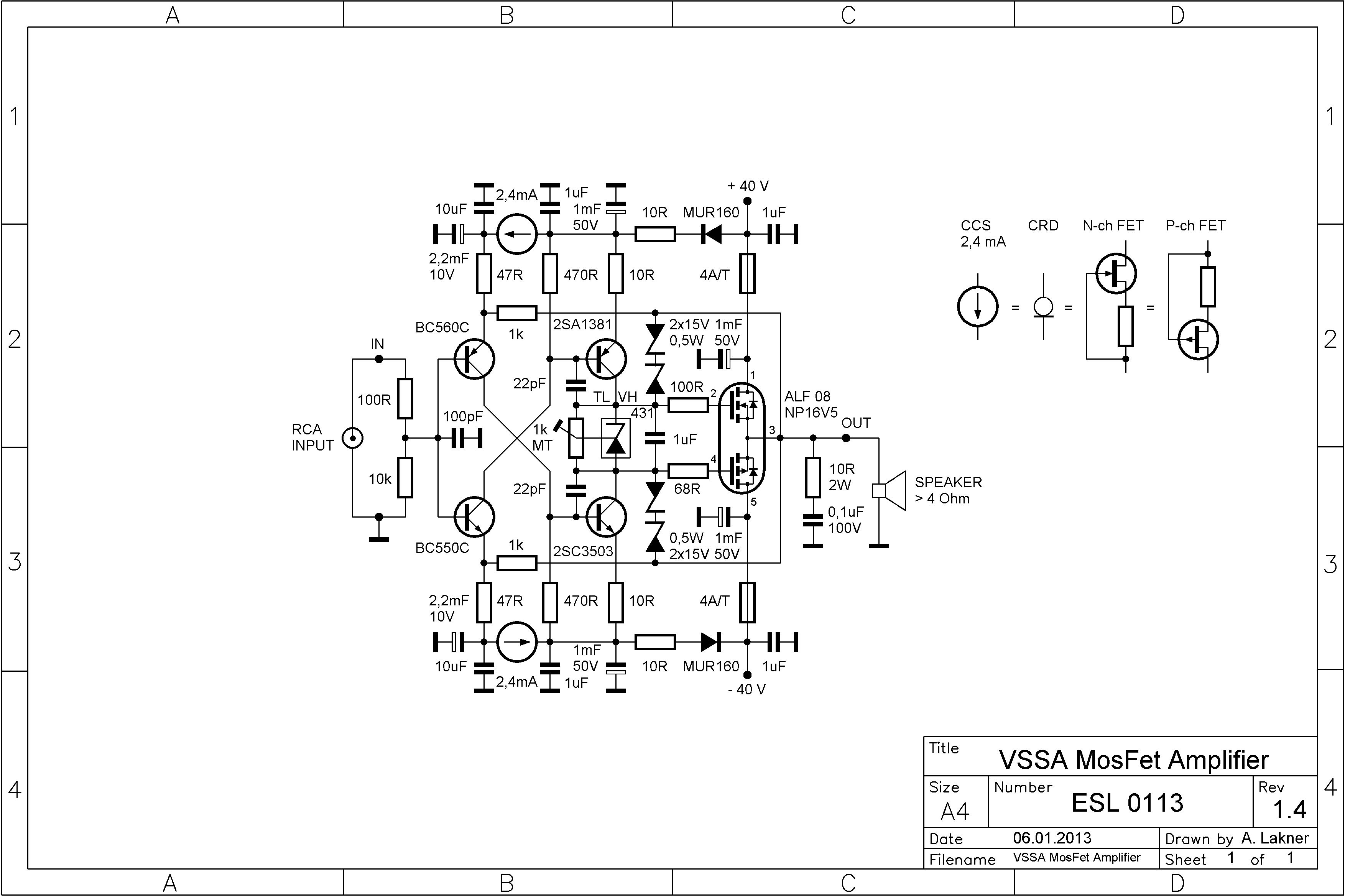
Struth, hundreds of VSSA, First ones etc... builds without any stability issues. They all have a 100pF directly from base to ground as an input filter. It does not introduce any instability, on the contrary, it kills any overshoot due to excessive fast edges on square waves.
http://www.diyaudio.com/forums/atta...ssa-lateral-mosfet-amplifier-vssa-sch-1.4.jpg
A base/gate stopper is used to protect the previous stage from the capactive load.
What is interesting is when you probe the stability of an amplifier the input filter can make a significant difference to the overall PM/GM.
Have seen oscillations (only in sims) in CFA style amps when changing the input filter value. The caveat is that these amplifiers were NOT well designed. They were my early attempts 😉
So there is no confusion. I am in no way suggesting your DVSSA is a bad design. In fact I like the DVSSA (and similar) topology. 🙂 Just putting an idea out there...
Paul
Yeah for the 1st version as a starting experiment with this CFA I would like to
use my already made OPS (3EF BJT) if possible, but just for lazyness reasons. 🙂
Anyhow I think it should work somehow (maybe with different C values of course)
even if it's not the ideal OPS setup like with MOSFETs which I dont have right now.
About the protoype:
To test the CCSs I put a 4R7 resistor series to each of the 1st stage EFs into the collector going to the rails.
It looks like it's working but if I measure the voltage on the 2nd stage collector resistors (200R at my version)
it doesnt change when I adjust the CCS trimpot... 🙁
What should be the process? Based on the spice sims I thought to increase the CCS
currents untill the VAS emitter resistor currents are about 10mA, this should be OK?
(I'am using BC546/556Bs in the front and 2sa1360/2sc3423 for the VAS.)
+1Have seen oscillations (only in sims) in CFA style amps when changing the input filter value.
Some remarks about compensation.
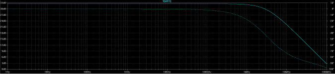
The first thing is to set the Miller cap, with NO input filter, in such a way that the amp is stable, with the highest bandwidth as possible, and no bump at HF in the response curve.
Once this is done, we gonna set the input filter between the two stages of the diamond in such a way that it has the hightest FC as possible, but kill any overshoot with fast square waves and little signals.
Now, we have an amp with the fastest slew rate you can achieve and no risk to overdrive its loops speed capacities.
And this filter isolate at HF the two stages of the diamonds with their tendency to instability, while the first stage isolate the filter form the input impedance source of your preamp. The FC will remain fixed what ever your preamp output impedance.
Time to set the input filter at the input of the first stage, to protect-it from RFI.
This i do, once in my system, with careful listening. A Ferrari that you drive at 60MpH 🙂 with no TIM possible.
One word about the Miller. I had set-it between the output of the power devices and the base of the VAS. It is because the power devices don't suffer from the current needed at HF to charge and discharge this cap. If you set-it, as we usually do, between collector and base of the VAS, the added charge for the VAS will increase distortion.
I'm totally unsure it will work stable if you add poles by current buffers in this local loop.
One word about the CSS. In the original VSSA, they are feeding the input transistor witch receive the feedback. In this situation, the are in the signal path of the closed loop. Here, they are on the first transistor of the diamond, witch is outside of the loop for signals. Reason why this input stage is faster with better phase margin. Slew rate matters in servo loops. Not when no global feedback.
i can't help you on this.Based on the spice sims I thought to increase the CCS currents untill the VAS emitter resistor currents are about 10mA, this should be OK?
I spend a lot of time on the bench to optimize both gains and currents in order to minimize distortions. My best results were with 1.5mA for each trannies of the diamonds, ~5.2mA for the VAS and ~ 145mA for the Laterals.
As both your output stage require a different polarization, and will behave in a totally different way, i fear you have to make all this work again from scratch.
The open loop gain is shared between the second stage of the diamond and the VAS. Both the overall gain and their relative ratio need to be optimized, as well as the currents for distortion.
"Simple" requires sometimes a lot of tuning ;-)
It is a totally different approach from the one of OS, where distortions are minimized by design, adding poles at the expense of speed or stability margins.
BTW: when you play with your CSS, don't forget to remove the servo ;-)
Last edited:
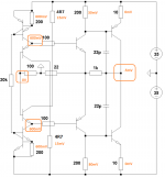
I just saw this answer right now.R1, R2 are meaningless, R9, R10 too large, C8 dangerous, Q1, Q4 buffer could degrade SQ. At the end all comes down to implementation, choice of parts, etc.
My comments:
R1, R2 are low values, comparing of the impedance of the CSS. No inconvenience expected. They allow to measure the currents on the bench (industrial reflex ;-), and gives a little isolation against parasitic capacitance. Dampen the Q.
R9, R10, agree, the reason why i used 100 and 80 for them in the definitive schematic ;-)
C8, agree, and was suppressed in the definitive schematic.
"Q1, Q4 buffer could degrade SQ". No ! Exactly the contrary, both in measurements and listenings.
The schematic used by jkuetemann was just a "theory of operation" before optimisation.
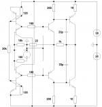
Definitive schematic was here: http://www.esperado.fr/vssa-diamond/dvssa.php

So if I get it right this layout should be stable just with the 2 miller caps without the first 3 filter caps?The first thing is to set the Miller cap, with NO input filter
FC = ?The FC will remain fixed what ever your preamp output impedance.
Please consider: I just connected this way for a start. Later I'd use it the same way (via the OPS) just as you did.If you set-it, as we usually do, between collector and base of the VAS, the added charge for the VAS will increase distortion.
I understand that, but I guess the algorithm should be the same.i can't help you on this.
I spend a lot of time on the bench to optimize both gains and currents
Or how did you set your VAS Iq? I guess the resistors for the 2nd stage and the VAS were fiexed, right?
If so, only the CCS can be adjusted to set the correct current, right?
Please help with the algorithm to bring this amp alive... 🙂
And how did you achieve this? Basically with spice or with real life distortion measurements?Both the overall gain and their relative ratio need to be optimized, as well as the currents for distortion.
DC servo isnt there at all now, I just prepared the possibility if needed later.BTW: when you play with your CSS, don't forget to remove the servo ;-)
Last edited:
Hehe, I never understood why didnt you answer them earlier, but finally you did it... 🙂I just saw this answer right now.
BTW I also didn't know this amp was built in eal life. Thought just a spice level PoC layout... 🙂
Oh yes. Depending of the board, devices etc... you can increase miller cap. I used 20 pF on my prototype. But BJT will behave differently.So if I get it right this layout should be stable just with the 2 miller caps without the first 3 filter caps?
Oh, more than 10MHz, it is just to avoid overshoot on square signal with fast edges and dump the diamond. Your real input filter will be the one at the first input. (that you will like at 200KHz ?)FC = ?
I did-it on SIM as first approach, too long in real life. Then verified on proto that it was not too far. When you set the currents, there is an optimal point for 1000 Hz distortions. Increase more, and the distortion at 1000 Hz increase, while 10000Hz decrease, but just a little.Or how did you set your VAS Iq? I guess the resistors for the 2nd stage and the VAS were fiexed, right?
If so, only the CCS can be adjusted to set the correct current, right?
And how did you achieve this? Basically with spice or with real life distortion measurements?
Try between 5 and 20ma of VAS current by adjusting the CSS currents. Is your SIM is working with your BJTs ?
Last edited:
FC : I meant the meaning of the letters.
Yes its working in spice! (with ideal trans).
So the VAS current should be set with the CCS right?
Yes its working in spice! (with ideal trans).
So the VAS current should be set with the CCS right?
1 - FC = "Frequence de coupure".(So sorry :-()1: FC : I meant the meaning of the letters.
2- Yes its working in spice! (with ideal trans).
3- So the VAS current should be set with the CCS right?
2- Can-you show-us the resulting frequency response, (AC analysis with no input filters) ?
3- Yes, of course. But you have to take care of the polarization of the output stage for your BJTs: 3X0.7V = ~ > 2.1V each side.
Temptation...
Hmmmm...
Esperado,
I have 4 pairs of Exicon ECW20x20s laying about (doing nothing)...
Have no intention of ever designing my own Lateral MOSFET amp but have everything needed to build 4 of these (DVSSA) including suitable PSU. 🙂
Was a DIY PCB layout ever made public?
If so, very tempted. 🙂
Paul
Hmmmm...
Esperado,
I have 4 pairs of Exicon ECW20x20s laying about (doing nothing)...
Have no intention of ever designing my own Lateral MOSFET amp but have everything needed to build 4 of these (DVSSA) including suitable PSU. 🙂
Was a DIY PCB layout ever made public?
If so, very tempted. 🙂
Paul
Tried it out: I removed the first 3 HF filter caps and kept just the 2 x 22pF miller caps at the VAS.
Now its not oscillating but I simply cannot set the currents and I don't get it why... 🙁
Based on the 4R7 resistors I put in the 1st stage EF collectors the CCS is working but there is no current even in the 2nd stages.
If I measure the voltage on their resistors while increasing the CCS current it doesnt increase but decreases after a while... 😕
The CCS is already at 5-6-7mA and nothing at the 2nd stage. I checked the whole PCB and measured all of the transistors and resistors but everything looks fine.
I don't think so.Hmmmm...
Was a DIY PCB layout ever made public?
You can start from The L.C. VSSA layout and modify-it ?
No mix between NPN and PNP of the diamond ?Tried it out: I removed the first 3 HF filter caps and kept just the 2 x 22pF miller caps at the VAS.
Now its not oscillating but I simply cannot set the currents and I don't get it why... 🙁
Based on the 4R7 resistors I put in the 1st stage EF collectors the CCS is working but there is no current even in the 2nd stages.
If I measure the voltage on their resistors while increasing the CCS current it doesnt increase but decreases after a while... 😕
The CCS is already at 5-6-7mA and nothing at the 2nd stage. I checked the whole PCB and measured all of the transistors and resistors but everything looks fine.
(You understand now, the interest of the resistance i put in serial between CSS and emitter of the first stage, to can measure currents ?)
Base of the first stage well referenced to the ground ?
If the answers are yes to those questions, time to incriminate your CSS.
First, ensure they both work properly.
Can-you show us the voltages at emitters of the first tranies ?
Last edited:
I checked again but no NPN-PNP mix.
Series CCS resistor: yes, it (would be) good now for testing..! 🙂
GND reference: yes, just as on the schematic.
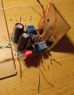
I measured a few voltages, the results are attached.
Poor DVSSA of mine slowly looks like a hedgehog... 🙂
CCS: if I increase the current the voltages are increasing nicely on the 4R7 resistors
up to 30-40mV (6-8mA...) but voltage on the 2nd stage 200Rs are not increasing... 🙁
CCS common 20k: I am not sure is this common resistor good this way or should be split up to 2 x 10k to GND?
In spice it works but that doesnt mean anything due to "super symmetry" based on ideal parts.
Series CCS resistor: yes, it (would be) good now for testing..! 🙂
GND reference: yes, just as on the schematic.
I measured a few voltages, the results are attached.
Poor DVSSA of mine slowly looks like a hedgehog... 🙂
CCS: if I increase the current the voltages are increasing nicely on the 4R7 resistors
up to 30-40mV (6-8mA...) but voltage on the 2nd stage 200Rs are not increasing... 🙁
CCS common 20k: I am not sure is this common resistor good this way or should be split up to 2 x 10k to GND?
In spice it works but that doesnt mean anything due to "super symmetry" based on ideal parts.
Attachments
Last edited:
I checked again but no NPN-PNP mix.
Series CCS resistor: yes, it (would be) good now for testing..! 🙂
GND reference: yes, just as on the schematic.
I measured a few voltages, the results are attached.
Poor DVSSA of mine slowly looks like a hedgehog... 🙂
CCS: if I increase the current the voltages are increasing nicely on the 4R7 resistors
up to 30-40mV (6-8mA...) but voltage on the 2nd stage 200Rs are not increasing... 🙁
CCS common 20k: I am not sure is this common resistor good this way or should be split up to 2 x 10k to GND?
In spice it works but that doesnt mean anything due to "super symmetry" based on ideal parts.
Hi,
Can you provide a drawing with all transistor voltages? There isn't enough information yet.
The common 20K on the CCS is fine. Tying the 10Ks to GND is suboptimal in that it requires an extra GND connection. I like to avoid GND connections wherever possible.
Keep going. You will get it working and learn a lot in the process. The harder the journey the sweeter the reward. 🙂
Paul
I don't think so.
You can start from The L.C. VSSA layout and modify-it ?
Hi Esperado,
That's an idea. It looks like a nice little project as a diversion from my "lunchtime amp". Been using my Leach amps for the past 10 years and would like a change. 🙂 But the lunchtime amp is so far away from completion....
May need some mods due to the double die output devices. Probably need an increase in bias current for the VAS, smaller gate resistor values and maybe an increase in miller compensation. None of this should be a problem.
Paul
May-be the simplest way should be to wait for the release of the next Lazy Cat First one ? I believe it will be the same kind of thing, diamond input with no cap anymore in the signal path and he promised-it for soon.May need some mods due to the double die output devices. Probably need an increase in bias current for the VAS, smaller gate resistor values and maybe an increase in miller compensation. None of this should be a problem.
I understood he will propose 3 versions with different powers.
I can't say more, the guy turned in a very strange commercial "fashion" attitude and don't share anything anymore on a technical way while we had real friendly relationship in the past and a lot of things in common in our design choices, methods and tastes.
This said, i'm sure his amp will be very good, as he his (was ?) a very good designer on my opinion.
My project was done for him, to try to convince him of the benefit of my modified diamond dumping idea. Because he used to say he don't like the "nervous" behavior of the diamonds. No more real communication between us any more since this moment :-(
Just stupid comments like "R1, R2 will drop 75 mV, in series with several M Ohms of CCS impedance will do exactly nothing". Stupid (I explained why) arrogant (he don't even asked why those resistances) and not friendly.
I'm disappointed and saddened.
Last edited:
Intresting: I tried up to 330pF miller caps but still it can go to oscillation easily
for example even when I just touch the rails with the DMM probe... (Input still shorted.)
BTW: it's not clear to me how the currents should be set up in the 2nd stage transistor?
The 1st stage and the 3rd (VAS) are clear: 1st: CCS current directly, VAS: 2nd stage resistor + the current on it.
But how the 1st stage should bias the 2nd stage? Let say BE voltage on 1st Tr = 550mV and should be 600mV
on 2nd stage Q how can this work? In spice of course they are 100% the same thats why its working I guess.
The 1st stage bases and the 2nd stage emitters are both on GND, right..?
Anyway I try to measure some voltages in the meantime... 🙂
Last edited:
Very strange. Think about-it. If the VBE of you NPN was so inferior to the one of your PNP, we could understand the second stage of the diamond (negative rail side) can not reach enough voltage to turn in. But, in this case, the opposite arrangement (PNP-> NPN, positive rail side) would present an opposite behavior, with a *lot* of current in the second stage.I checked again but no NPN-PNP mix.
Series CCS resistor: yes, it (would be) good now for testing..! 🙂
GND reference: yes, just as on the schematic.
I measured a few voltages, the results are attached.
Poor DVSSA of mine slowly looks like a hedgehog... 🙂
CCS: if I increase the current the voltages are increasing nicely on the 4R7 resistors
up to 30-40mV (6-8mA...) but voltage on the 2nd stage 200Rs are not increasing... 🙁
CCS common 20k: I am not sure is this common resistor good this way or should be split up to 2 x 10k to GND?
In spice it works but that doesnt mean anything due to "super symmetry" based on ideal parts.
Diamonds are nothing new, thousands of them working everywhere.
(Some even said there are eternal ;-)
So, you made a mistake in cabling somewhere, verify from scratch.
About your 20K, nothing to fear from the ~4mA it will carry to the earth in case you set 2X10K to ground. Just you can chose your evil between common mode and differential mode PSRR.
With your CSS typology, the value of the adjustable resistance to feed 1.55mA to the input transistors is simulated around 420 Ohms in my LTSpice.
Last edited:
- Status
- Not open for further replies.
- Home
- Amplifiers
- Solid State
- Evolution of the VSSA? Esperado's DVSSA...