Just putting diamond buffer alone as input stage in VSSA will not do miracles, more important is its practical implementation, which has to be flawless, meaning using very good CCS, ...
Yes, I agree. In my effort to better VSSA with diamond buffer, I can only come up with different result (as shown by my first picture of FFT charts), which I will still prefer no diamond option. But with extra other transistor as shown below, DVSSA doesn't have weakness with the input stage, therefore the performance can be made outstanding. I think that will be my next step from VSSA.
Attachments
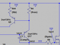
I see, nested local feedback for input CCS. Be careful, in a manner of DC bias conditions, this one's having PTC character.
I see, nested local feedback for input CCS. Be careful, in a manner of DC bias conditions, this one's having PTC character.
Thanks for the warning. A diode in series with R4 might solve issues but I haven't started yet. Still finishing on going project(s).
Hi Guys!
I'd like to build my very first CFA/VSSA at last... I'm very curious to the outcome and waitng for the adventure... 🙂
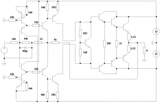
I read a lot of threads and I'd start with this layout based on Esperados recommended design.
Every suggestions are warmly welcomed and thanks in advance!
BTW: shall I put my later "blog" with this layout in this thread?
Targets/features:
Questions:
Any comments are welcomed!
Cheers!
I'd like to build my very first CFA/VSSA at last... I'm very curious to the outcome and waitng for the adventure... 🙂
I read a lot of threads and I'd start with this layout based on Esperados recommended design.
Every suggestions are warmly welcomed and thanks in advance!
BTW: shall I put my later "blog" with this layout in this thread?
Targets/features:
- VSSA topology
- diamond input (no ugly caps @ FB)
- no input series C (DC servo if needed as "2nd floor module" attached to main PCB)
- 60V DC PS
- C multiplier for whole IPS
- max Iqs possible (motto: I (and BJTs) love high currents... 🙂)
~5mA for input stage and ~15mA for VAS - Qs: BC546B/BC556B + 2SC3423/2SA1360 (or similar...)
- BJT EF3 for 1st OPS version (that's on my prototype board already 🙂)
- very compact PCB
Questions:
- starting schematic is ok?
- starting pcb is ok?
- advices to start HF comp..?
Any comments are welcomed!
Cheers!
Attachments


Hi Guys
Wasn't LC's circuit essentially four devices to begin with? Very much like a "de-evolution" of the CFA - make it as simple as possible but still work and possibly perform to some subjective standard.
This thread is a standard CFA and nothing new.
Have fun
Wasn't LC's circuit essentially four devices to begin with? Very much like a "de-evolution" of the CFA - make it as simple as possible but still work and possibly perform to some subjective standard.
This thread is a standard CFA and nothing new.
Have fun
This is a DVSSA thread. Why do you mind trying it out?
BTW: I didnt find a post with the results of a real life dvssa.
And having the smallest numbers of devices are not surely the best solution.
BTW: I didnt find a post with the results of a real life dvssa.
And having the smallest numbers of devices are not surely the best solution.
I'm waiting a long someone to do this DVSSA!Hi Guys!
I'd like to build my very first CFA/VSSA at last... I'm very curious to the outcome and waitng for the adventure... 🙂
I read a lot of threads and I'd start with this layout based on Esperados recommended design.
Every suggestions are warmly welcomed and thanks in advance!
BTW: shall I put my later "blog" with this layout in this thread?
Targets/features:
- VSSA topology
- diamond input (no ugly caps @ FB)
- no input series C (DC servo if needed as "2nd floor module" attached to main PCB)
- 60V DC PS
- C multiplier for whole IPS
- max Iqs possible (motto: I (and BJTs) love high currents... 🙂)
~5mA for input stage and ~15mA for VAS- Qs: BC546B/BC556B + 2SC3423/2SA1360 (or similar...)
- BJT EF3 for 1st OPS version (that's on my prototype board already 🙂)
- very compact PCB
Questions:
- starting schematic is ok?
- starting pcb is ok?
- advices to start HF comp..?
Any comments are welcomed!
Cheers!
Congratulations Cortez!
I'm just working on my v2.0 advanced symasym but after that (hopefully in a few days) I'll build this dvssa!
Any comments for the starts? HF comp. strategy? Or the Esperado's version will be good for a start?
Other: I saw at the CF-FET thread that a simple CC buffer is used right before the VAS.
Can this improve something even with a BJT VAS..? Any comments? Worth a try..?
I know... slowly I have to remove the letter "V" from the "dvssa"... 🙂
Hi Guys
Cortez: I think the first S needs removal too. Doesn't it stand for "simple" ? (V for 'very')
You can eliminate the big caps in the feedback loop by adding an input structure that in most situations looks like a diamond, but the input BJTs are wired as diodes rather than gain elements. Feedback is applied just as with the diamond, so it is DC. Some opposed to diamonds promote this diode structure.
You lose the current gain and thus some DC accuracy. Others here have used that input wiring. Using 1N914s works nearly as well as diode-wired BJTs. The latter has some nuance of advantage and a definite aesthetic appeal.
I am not advocating simplicity for simplicty's sake. Rather, pointing out the common human "new wheel" effect that occurs all the time. When you approach a given study from a different angle you initially believe it to be an entirely different study than you first saw. As "refinements" are added the result ends up being something that already exists. All the schematics on this thread are just the standard CFA. Each builder can call his construction of it something unique but the topology is that standard.
I have great respect for Esperado, and you Cortesz, and for the others here. LC's circuit eliminated an input cap but still has caps in the signal path. This thread's goal is to eliminate the caps in the feedback path, too, but it still does not eliminate caps from the signal path entirely. No amp here can or does. How can you make a power supply without caps?
Have fun
"Diodemond": thanks Struth, I'll try this both in LT and in real life.
BTW: is there some simple reason not to use a diamond or its just a belief..?
Or why is this diodemond better?
"New wheel": my purpose is not something new just try out a (standard) CFA for the first time.
I like the VSSA as well but I thought to begin with a little more advanced version.
BTW: if I am right LC's First one is moving to this direction as well with time.
Caps: of yourse but while you can remove them from the FB path you cannot from the PS... 🙂
Hi Guys
I believe it was on one of Dadod's threads that a discussion of diamond vs diode-wired inputs occurred. I know krglee calls diamonds "evil". I don't think they are quite that bad and would rather use the diamond than the diode-wired devices, since to me the current gain afforded is useful for DC accuracy and to provide a higher input impedance.
Most things evolve in a circular way. Simplifications often cause reduction of performance. It is up to each builder to decide what level of THD is acceptable, or what bandwidth is best, or if distortion profiles are more important than absolute values. If we try "simpler" and see bigger THD, then we try what the simpler topology allows as a way to get THD as low as it can be, then find we do not have "simple" anymore.
Of course, "simple" is relative. a 14-device circuit is simple to some and too much to another.
Have fun
I'm just working on my v2.0 advanced symasym but after that (hopefully in a few days) I'll build this dvssa!
Any comments for the starts? HF comp. strategy? Or the Esperado's version will be good for a start?
Other: I saw at the CF-FET thread that a simple CC buffer is used right before the VAS.
Can this improve something even with a BJT VAS..? Any comments? Worth a try..?
I know... slowly I have to remove the letter "V" from the "dvssa"... 🙂
Cortez /struth .... I already went to esperado's site - seeked his advice -
it's been built /tested and now goes to through hole (even SMD).
It has NO issues , it's the most perfect of the CFA's in every way.
Cortez - look to the slewmaster NAD as the simple version and the
new Kypton ND as the "fancy version" - both are tested /with scope shots,
overload ... everything.
OS
I'm waiting a long someone to do this DVSSA!
Congratulations Cortez!
You just built it , thimios ??
OS
Cool, thanks Pete!Cortez - look to the slewmaster NAD as the simple version and the
new Kypton ND as the "fancy version" - both are tested /with scope shots,
overload ... everything.
OS
Just to confirm these are the tested versions?
Simple: http://www.diyaudio.com/forums/solid-state/248105-slewmaster-cfa-vs-vfa-rumble-11.html#post3831104
Fancy: http://www.diyaudio.com/forums/solid-state/248105-slewmaster-cfa-vs-vfa-rumble-629.html#post4205853
BTW: Lazy Cat and Esperado did spot/mention something with this layout about FB impedance vs phase shift (wrong RC config).
Is it still so or these configs are already advanced ones..?
First, setting the input low pass filter between the emitter of the first transistor and the second of the diamond really gives an improvement, as it bring both a FC insensible to the source impedance, and kill the tendency of the Diamond to oscillate. (on my opinion and listening tests).[*]starting schematic is ok?
[*]starting pcb is ok?
[*]advices to start HF comp..?
Second, about compensation, try, if you can, to set-it between output of the power transistors and base of the VAS. It reduce distortion because the output has a great current margin to afford the charge of this condenser at very HF.
it is better than between its base and collector.
Third, try to optimize the gain of the second stage of the Diamond, testing various combinations for minimal distortion. Simulators helps a lot here.
Last, set your compensation cap value with no input filter for a max flat response curve at HF (no peak). Then set a minimal input filter just enough to kill any overshoot with little signal square waves.
My two cents.
Last edited:
About impedance of the FB, If you increase-it, it reduce the Bandwidth and increase distortion at HF. This is due to the non linear parasitic capacitance of the emitter of the input stage. There is a minimal value under it will not change anything. Stay a little under this value, your are done.
Don't forget that the serial resistance will pass big currents and is critical in regard to the sound quality. Don't hesitate to chose the best you can (non magnetic, not inductive) and to oversize-it.
Don't forget that the serial resistance will pass big currents and is critical in regard to the sound quality. Don't hesitate to chose the best you can (non magnetic, not inductive) and to oversize-it.
Last, please, don't believe that the L.C. VSSA or my Diamond VSSA are primitive, because they look simple.
The goal was to minimize the number of poles and zeros, in order to have a rock solid amp. The final schematic is the result of hours of optimizations at each and every place to get a minimal distortion figure, well under audibility threshold, despite the simplicity. A more time consuming work than adding complexity.
OS had a different approach, adding drivers or Baxandall VAS, with amazing results on the paper. I am very passionate about the idea to compare the two approaches, in listening, to make myself a philosophical opinion.
transparency VS distortion free ;-)
I will build a Lateral mosfet version of one of his CFA as soon as possible to do this. (I stick with them ;-)
Thank you Esperado your notes are really appreciated!
http://www.esperado.fr/vssa-diamond/dvssa.php
This means there is no need for C3 but just for C11/12..?
BTW: which parasitic C is worse: feeding the base of a transistor or the E with the FB signal?
(Assuming same R values in the FB network...)
I'm not sure I get it right. Based on your schematic here:First, setting the input low pass filter between the
emitter of the first transistor and the second of the diamond really gives an improvement,
as it bring both a FC insensible to the source impedance, and kill the tendency
of the Diamond to oscillate. (on my opinion and listening tests).
http://www.esperado.fr/vssa-diamond/dvssa.php
This means there is no need for C3 but just for C11/12..?
Ok, but how this minimal value can be defined..?About impedance of the FB, If you increase-it, it reduce the Bandwidth and increase distortion at HF.
This is due to the non linear parasitic capacitance of the emitter of the input stage. There is a minimal
value under it will not change anything. Stay a little under this value, your are done.
BTW: which parasitic C is worse: feeding the base of a transistor or the E with the FB signal?
(Assuming same R values in the FB network...)
My point is to set the low pass filter C11/12, as i indicated. Free to add, if necessary an other one before input for RFI immunity and ultimate protection against TIM. At much lower FC (250K ?) that you can adjust in listening in your system because it depend of the impedance of the source and your speakers too.I'm not sure I get it right. Based on your schematic here:
http://www.esperado.fr/vssa-diamond/dvssa.php
This means there is no need for C3 but just for C11/12..?
The easier is to simulate or measure the bandwidth in closed loop. Because it depends of the input transistors you'll use.Ok, but how this minimal value (of feedback impedance) can be defined..?
Last edited:
- Status
- Not open for further replies.
- Home
- Amplifiers
- Solid State
- Evolution of the VSSA? Esperado's DVSSA...