An analogy used by Gootee that I have stolen goes as follows:
Imagine the HF decoupling cap, on each supply rail, is the sole supply of energy and further imagine them as batteries that will exhaust themselves in 1us.
Now wire the active device so that the current from the HF cap can get into and out of the device and back to the cap in the shortest possible distance. 2 to 3mm for Total Loop Length is possible and should be the target for this HF decoupling.
Work with 20mm as the target for Total Loop Length for the MF decoupling since this time the caps deplete in 20us.
The PSU's job is simply to recharge the two sets of "battery" equivalent decoupling capacitors.
An analogy used by Gootee that I have stolen goes as follows:
Imagine the HF decoupling cap, on each supply rail, is the sole supply of energy and further imagine them as batteries that will exhaust themselves in 1us.
Now wire the active device so that the current from the HF cap can get into and out of the device and back to the cap in the shortest possible distance. 2 to 3mm for Total Loop Length is possible and should be the target for this HF decoupling.
Work with 20mm as the target for Total Loop Length for the MF decoupling since this time the caps deplete in 20us.
The PSU's job is simply to recharge the two sets of "battery" equivalent decoupling capacitors.
Hmm that is an interesting analogy.
But if these decoupling caps are connected between each rail and ground, and you want to get "into and out of the IC and back to the cap in the shortest possible distance" but there is no ground connection with the IC, then you must form a loop to where ever the output of the IC is headed. Or am I missing something here...
Also, am I incorrect to assume this mandates a bypass cap between ground and every PS power pin of each IC on the entire board?
The Power supply loop from the decoupling cap into the chip and back out of the chip must be minimised.
Sometimes that loop must include the HF load and a virtual ground AT THE CHIP.
Follow where the current must go and give it a route back to the source of the current. This is the route that MUST be very short.
Sometimes that loop must include the HF load and a virtual ground AT THE CHIP.
Follow where the current must go and give it a route back to the source of the current. This is the route that MUST be very short.
Input and output connectors are better placed at the same side of the board.
A common mode current flowing in your cable shields will then go from one connector to the other and not though the whole board.
Good point. In general I can see that this is good advice.
In this case, the circuit is for a headphone amplifier. Ground loop currents will only enter the board at the inputs and will not flow through the board. This is why I used a separate return for inputs and outputs.
When any device changes state it requires a supply of energy, it takes a finite amount of time for this energy to flow from the main PSU to each device, due in part to the inductance or the connection from the devices to the main PSU. So you use decoupling capacitors to effectively lower this inductance by supplying instantaneous current requirements. Think of it as a bucket brigade, with the local decoupling capacitors (small both in value and physical size to minimise parasitic inductance) providing the instantaneous current, these then being filled from the main supply reservoir capacitors (usually large value electrolytics). So we have split the design into two current loops, one the local decoupling loop, the second being between the main PSU reservoir caps and the local decoupling....Now if you take the GND side of the local decoupling caps back to the main PSU caps all you are doing is creating a bigger loop and effectively making the local caps useless for the purpose they were put there.
There is a very good paper by Xylinz regarding decoupling Virtex devices (OK it high speed digital, but it does explain better than I can how the energy is supplied from the SLOW main PSU to each level of fasted decoupling, again Andrew uses some good terminology regarding this with fast medium and slow, but I'll let him elaborate).
Add further to this problem the good chance of picking up noise from the environment, mobile phones, wireless networks, mains born communication's etc. and you have to start thinking seriously about RF layout especially for low level signals, where this interference will be more noticeable and critical to signal integrity.
This is basically the same as Andrew has said above, in a tiny bit more detail.
At audio frequencies this is quite critical, once you start delving into analogue/digital or digital decoupling becomes critical to the circuitry working correctly.
Good point. In general I can see that this is good advice.
In this case, the circuit is for a headphone amplifier. Ground loop currents will only enter the board at the inputs and will not flow through the board. This is why I used a separate return for inputs and outputs.
They are still join though, this is getting into EMC engineering territory, there are some excellent papers regarding this on this site, including a couple of AES presentations, recommended reading.
http://www.hottconsultants.com/
Originally Posted by CharlieLaub
The bypass caps at the ICs.
Have another look at my earlier screenie, & you'll see that NO bypass caps are DIRECTLY connected to Common/Ground, only via their own returns to the the PS Star point.
People can choose to do whatever they want, but i would say, build 2 otherwise identical circuits, one as others are suggesting, & one as i have. Then both listen & test & discover which you prefer ! I know which i do, & listen to daily.
Are you referring to bypass caps at the ICs or PS reservoir caps in the above statement???
The bypass caps at the ICs.
See why I am confused here?
Have another look at my earlier screenie, & you'll see that NO bypass caps are DIRECTLY connected to Common/Ground, only via their own returns to the the PS Star point.
People can choose to do whatever they want, but i would say, build 2 otherwise identical circuits, one as others are suggesting, & one as i have. Then both listen & test & discover which you prefer ! I know which i do, & listen to daily.
Originally Posted by CharlieLaub
The bypass caps at the ICs.
Have another look at my earlier screenie, & you'll see that NO bypass caps are DIRECTLY connected to Common/Ground, only via their own returns to the the PS Star point.
People can choose to do whatever they want, but i would say, build 2 otherwise identical circuits, one as others are suggesting, & one as i have. Then both listen & test & discover which you prefer ! I know which i do, & listen to daily.
I went back to the "screenie" and I think it makes more sense now that there have been other related posts that are trying to hammer home various points.
Let me ask you this, when you have to run so many separate common/ground returns, what's the relative importance of track/trace length and width? Can they be as thin as e.g. 10mils?
I think that as regards rail-to-rail decoupling, we should remember that there is a low-impedance AC path to ground from either rail through the PSU (voltage sources).
I think that as regards rail-to-rail decoupling, we should remember that there is a low-impedance AC path to ground from either rail through the PSU (voltage sources).
That's fine if connections between power supply source and rest of circuit are short.
It doesn't take a lot of current to start modulating the ground line.
I always use local decoupling as well.
Good point. In general I can see that this is good advice.
In this case, the circuit is for a headphone amplifier. Ground loop currents will only enter the board at the inputs and will not flow through the board. This is why I used a separate return for inputs and outputs.
Many portable FM radios use the headphone cable as an antenna... no matter what you do it will pick up radio signals as common mode. It is better not to allow these to run through your board.
Originally Posted by CharlieLaub
I went back to the "screenie" and I think it makes more sense now
Good
Can they be as thin as e.g. 10mils?
For low current stuff, i'ld say that even 1mm should be more than fine.
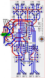
I have just been having a look at that board in post 22, and I feel it has a few issues.
Lets start at the output end of the thing:
Current flows to the load, then back to the load ground pin, fine, but now what?
Well it snakes across the board eventually ending up at that spider in the middle, now where to?
Well if the load is swinging positive the loop closes via a skinny trace to the opamp positive rail decoupling cap (C12) and hence to the positive supply pin (Some will also go via C19 and the positive rail), the rail to rail decoupler does us no good in this situation becase there is no direct way for the ground current to get to it.
Driving the load negative however has a bit of a problem, the caps to get back to the negative rail are C13 & C20 which are next to the gain control chip, not the output driver....
Further there is a common impedance between all the outputs (The track back to the star point) so there will be crosstalk.
Much better IMHO would be to put a local star point under the output opamp connecting the output grounds, and decoupling caps for both the opamp rails together at this point (This can then connect to your main ground (seeing as you lack a plane).
R32 - R35 connect (via another common impedance!) to the star point, would they not be better connected to whichever pin the gain control chip uses for its input reference (And from there to the star point if you really must)?
The opamp non inverting pins connect (more or less) to the VCA reference, which is sane, but the blue trance from pin 5 cold usefully just run under the chip to pin 10?
C28 is UNDER the VCA, you have plenty of space, why do this?
The star point by the rectifier for the cap charging curent pulses is probably a good thing.
Given the thing is a VCA you may want to cap couple the inputs to remove any DC offset.
You are aware that the 2164 is obselete?
Regards, Dan.
Thanks for your post and analysis. I wanted to follow up. See below. I have attached part of the layout with some labels, which I hope will make some things clearer.
As I mentioned before, I return input and output traces to the left side of this GND star, and I take the reference common/ground from the right end of the star. Not shown in this view is the connection between this star and the star of the smoothing caps common, which leaves at the left extreme of the GND star shown.
This is a 2-layer analog only board. I only had room for so many traces, and this puts limits on where I can put stars, power traces, ground returns, etc. Its a compromise.
I have a separate return to the ground star for the input ground return via R32,R33, R34, R35 in case there is a ground loop type situation. My thought was that this would keep that current from polluting the ground reference for the two ICs, but maybe that is the wrong approach since it forms a longer path to the ground pin (yes explicit ground pin on SSM2164, shown in green as "GND").
You are correct about the common return (at least a portion of it) for the output common/ground returns, but again there was not enough space for two. I didn't think of this at the time, so thanks for pointing it out. I can measure the crosstalk after I build the board.
C28 is a rail-to-rail decoupling cap. It's optional, and because of space constrains I put it underneath to keep leads as short as possible. I may not install it at all.
Good thought about the DC blocking cap on the VCA. I'm not too worried about this for now. In my initial application this board is driven by a transformer-coupled output, so no DC. Also, the VCA can handle DC offset fine, although I should test to see if this effects the distortion levels...
Actually the 2164 is not obsolete. It's being produced by Cool Audio currently as the V2164. The original ICs from AD are still easy to find as well.
Let me know if you have more questions or there are things that I can clarify. You've brought up some good points. Thanks.
Looking at the attached partial layout you can see that I have removed most of the power supply. What is left of it are the two capacitors on the output of the regulators and the main audio star ground. I consider this to be all that is relevant to the power related issues.I have just been having a look at that board in post 22, and I feel it has a few issues.
Lets start at the output end of the thing:
Current flows to the load, then back to the load ground pin, fine, but now what?
Well it snakes across the board eventually ending up at that spider in the middle, now where to?
Well if the load is swinging positive the loop closes via a skinny trace to the opamp positive rail decoupling cap (C12) and hence to the positive supply pin (Some will also go via C19 and the positive rail), the rail to rail decoupler does us no good in this situation becase there is no direct way for the ground current to get to it.
Driving the load negative however has a bit of a problem, the caps to get back to the negative rail are C13 & C20 which are next to the gain control chip, not the output driver....
Further there is a common impedance between all the outputs (The track back to the star point) so there will be crosstalk.
As I mentioned before, I return input and output traces to the left side of this GND star, and I take the reference common/ground from the right end of the star. Not shown in this view is the connection between this star and the star of the smoothing caps common, which leaves at the left extreme of the GND star shown.
This is a 2-layer analog only board. I only had room for so many traces, and this puts limits on where I can put stars, power traces, ground returns, etc. Its a compromise.
I have a separate return to the ground star for the input ground return via R32,R33, R34, R35 in case there is a ground loop type situation. My thought was that this would keep that current from polluting the ground reference for the two ICs, but maybe that is the wrong approach since it forms a longer path to the ground pin (yes explicit ground pin on SSM2164, shown in green as "GND").
You are correct about the common return (at least a portion of it) for the output common/ground returns, but again there was not enough space for two. I didn't think of this at the time, so thanks for pointing it out. I can measure the crosstalk after I build the board.
Much better IMHO would be to put a local star point under the output opamp connecting the output grounds, and decoupling caps for both the opamp rails together at this point (This can then connect to your main ground (seeing as you lack a plane).
R32 - R35 connect (via another common impedance!) to the star point, would they not be better connected to whichever pin the gain control chip uses for its input reference (And from there to the star point if you really must)?
The opamp non inverting pins connect (more or less) to the VCA reference, which is sane, but the blue trance from pin 5 cold usefully just run under the chip to pin 10?
C28 is UNDER the VCA, you have plenty of space, why do this?
The star point by the rectifier for the cap charging curent pulses is probably a good thing.
Given the thing is a VCA you may want to cap couple the inputs to remove any DC offset.
You are aware that the 2164 is obselete?
Regards, Dan.
C28 is a rail-to-rail decoupling cap. It's optional, and because of space constrains I put it underneath to keep leads as short as possible. I may not install it at all.
Good thought about the DC blocking cap on the VCA. I'm not too worried about this for now. In my initial application this board is driven by a transformer-coupled output, so no DC. Also, the VCA can handle DC offset fine, although I should test to see if this effects the distortion levels...
Actually the 2164 is not obsolete. It's being produced by Cool Audio currently as the V2164. The original ICs from AD are still easy to find as well.
Let me know if you have more questions or there are things that I can clarify. You've brought up some good points. Thanks.
Attachments
My point really is that you don't return current from the output to the ground star, you return curent from the output to one or the other of the opamp power pins, doing it via the star ground just provides a noise coupling path.
Currents flow in loops....
Seen in those terms there is nothing stopping you placing a local ground 'star' at the bottom of the page between the opamp and the output pins and connecting the output grounds and a pair of caps to the opamp power pins to it (Do it on the red routing layer you have loads of space), this local 'star' can then go to the main star ground via a small track as it caries little current).
This shortens the loop for output current, and keeps the switching current at crossover away from the input stage.
In this I find myself respectfully disagreeing with D.Self, you get away with rail to rail for 5532s when the load is well behaved, but I have seen it go very wrong on occasion with other parts.
You still show the input ground as connecting to the star point, but what is important is what the voltage between the top and bottom of R5 - R8 is and the virtual earth reference for the VCA is pin 8, so surely this should be the input reference point.
Looking at your routing sizes, you do know that 0.2mm track and gap is entirely routine these days (And 0.15 raises no issues)?
Also what is with the size of those caps, 0.3 pin spacing? 0.1mm spacing C0G for the < 1nF would be just fine and will again reduce your loop areas.
Disclaimer, I spent last week chasing 120dB of dynamic range at work (Currently -112dBFS is as good as the board I am using gets mostly due to layout issues (Not mine), that last few dB is a pain), return current issues make me twitch.....
Regards, Dan.
Good
For low current stuff, i'ld say that even 1mm should be more than fine.
ADDED INDUCTANCE makes the caps at the device pins useless....Small loop areas.
Why have you connected the 4 input grounds together, the 4 output grounds together, the 4 HF filter grounds together and the 4 -IN(opamp) together?
Don't you agree that it would be better to first connect the grounds per channel together, with each channel's output ground connecting to star ground.
Would it not be better to use 4 separate opamps?
Don't you agree that it would be better to first connect the grounds per channel together, with each channel's output ground connecting to star ground.
Would it not be better to use 4 separate opamps?
- Status
- Not open for further replies.
- Home
- Source & Line
- Analog Line Level
- understanding source+return current flow on PCBs