Not that you were trying to be patronizing in your response, but you are really dumbing this down a little too much with the train-on-track analogy!
I am not trying to be patronising, I have spent quite a lot of time trying to provide information that (as I don't know exactly what you understand regarding this) that will be helpful without being too complex, and no I am not dumbing it down, it is surprising how many think that electrons whizz round the wires ate high speed and how many don't understand how currents flow and how return currents work.
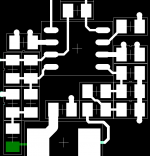
OK, I will just post the layout that I created so that it can be critiqued here in terms of grounding and signal routing. Please refer to the attached pic when reading the following.
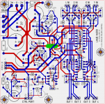
The power supplies for the circuit are found on the left side of the board. Starting at the top left corner, this consists of AC input (e.g. 18-0-18 Vac), rectifier, and smoothing caps connected to the 0V board input at a star point and arranged to form a CRC filter with R24 and R25. A single lead connects this star point with the main regulated ground star point, in center, light green color. The board uses LM317/337 regulators to create the +/- rails for the PS (e.g. 15V) plus an auxiliary 5V supply needed for the circuit at the bottom left of the board (The control input for the VCAs). The regulators use a small cap on the adjust pin to reduce noise. There are caps on the regulator output, 220uF elcaps (C19, C20). There are additional smaller caps (1uF MLCC) to the right of these (C12, C13) between the rails and ground as well as caps closer to the PS pins of the IC between rails (C11, C25).
I have tried to put some thought into the grounding scheme, and this was the impetus for creating this thread. I am aware that sometimes ground loops cause large circulating currents between boards and I have inserted some resistors on the input ground/shield lines that should reduce these currents. These are R32, R33, R34 and R35. I also ran a separate track back to the star ground point for these grounds to keep any remaining currents from polluting the ground reference used for the ICs, which is run as the large (red) track that emerges from the right end of the green star ground point. This leads up to the only ground (to right on IC) pin of the SSM2164 IC. This "IC ground" is split around this IC and ground tracks run down along each side to the ground pins of the lower IC (an OP482/TL074B). This was done to run the ground along side of the signal tracks between the two ICs, of which there are four, and to allow currents that return via these ground tracks from IC2 to IC1 to follow closely to the signal tracks. Finally, the ground/shield for the outputs is run separately from the IC ground reference from the green star ground down to just below the lower IC and then out to the board edge along the output tracks from the lower IC.
Please comment on this scheme, point out any mistakes and suggest improvement if you see any obvious ones. I have already sent this layout to the fab, and I will build it up when it arrives and then test it like I have done in this thread for an earlier version of this circuit:
Some tests on an earlier version of this circuit
Thanks.
Attachments
Last edited:
@ CharlieLaub
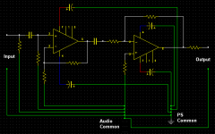
Hi, i would have used more colours, & more appropriate ones, in your PCB screenie, which might have made it a bit easier to follow etc 😉 Eg, ORANGE = AC, RED = V+ BLACK = V- GREEN = COMMON
I've mentioned before in other threads, that EACH component common connection should ideally have it's OWN trace returned to a central star point on the PCB. Also the PS should have it's own star point, which is then connected to the above star point. The audio input/output commons are connected to that.
I've never had Any issues doing that, & always get the best performance 🙂
actually the literal "star" with a squashed spider of traces is a poor approach - hierarchical gnds, segregating, ordering connections of noisy/dirty PS&gnd and clean gnds, minimizing loops, planes in low current Class A signal level regions generally does better
@ CharlieLaub
Hi, i would have used more colours, & more appropriate ones, in your PCB screenie, which might have made it a bit easier to follow etc 😉 Eg, ORANGE = AC, RED = V+ BLACK = V- GREEN = COMMON
This is not a colored schematic, it's the board layout. Red = bottom layer, blue = top layer. Things are color coded that way for a reason. Using the description I provided it should be pretty easy to follow... I'm just not going to spend hours recoloring everything by signal and I don't know of an automatic way to do that in my software.
I've mentioned before in other threads, that EACH component common connection should ideally have it's OWN trace returned to a central star point on the PCB. Also the PS should have it's own star point, which is then connected to the above star point. The audio input/output commons are connected to that.
I'm not exactly sure what you mean by "component common connection". What are you referring to there?
I think I am doing the star+star thing you mention to some degree. There is a star (red, towards upper left area) from the main smoothing caps and CRC filter. Then there is another star below the green area bear the center, which is where the ground for the regulated supplies connect. Also, I have run a bunch of separate ground returns back to the (green) star ground as I described, and segregated "dirty" and "clean" connections across the star. The green area indicates where the solder mask should not be applied so that one can build up this area with metal if desired.
I do agree with having separate planes and I am against these spider legs style star grounds, the ONLY place I have ever seen them is on DIY audio designs.
I have had a quick look at the design and will look in more detail later today, a schematic would be helpful though.
My first comment is all your Input returns join together and thus are summed back to the star point, each of these would be better going to their respective IC's and then to the star.
As I have said on many other threads, a ground plane will give better results and is more forgiving especially if people don't fully understand return currents. Spider leg star grounds are high inductance (both resistive and inductive) and add greater loops between the signal wire and the return, plus you cant always guarantee where your return is going to flow.
I do agree with zero Ds comment on having different colours for different nets, I will put up an illustration when I get to work.
@ CharlieLaub
Ok, but it'd be easier/qicker for people to follow if it was showed as i suggested. Anyway it's done now, but in future 😉
Any & Every component including wire screens etc etc that require a common/ground connection. So All audio ones have their own star, & All PS ones do, then joined Only between the two stars. Then Only the PS is actually Earthed. The chassis/case can then connect to the PS star. See my screenie as a simple example.
This is not a colored schematic, it's the board layout
Ok, but it'd be easier/qicker for people to follow if it was showed as i suggested. Anyway it's done now, but in future 😉
I'm not exactly sure what you mean by "component common connection"
Any & Every component including wire screens etc etc that require a common/ground connection. So All audio ones have their own star, & All PS ones do, then joined Only between the two stars. Then Only the PS is actually Earthed. The chassis/case can then connect to the PS star. See my screenie as a simple example.
Attachments
YUK. All you are doing is adding unnecessary parasitics to the layout in the return paths....
Last edited:
Regarding pretty colours on screen, I always colour my power and ground nest with pretty colours when doing a layout so I can easily identify them, GNDs in shades of green, power in whatever colour mood I am in.
4 supplies AGND and DGND (HDI construction PCB in this case, microvias)
4 supplies AGND and DGND (HDI construction PCB in this case, microvias)
Attachments
YUK. All you are doing is adding unnecessary parasitics to the layout in the return paths....
Yes, in general using single star grounds is at best a wobbly crutch, mostly to avoid the necessity of understanding exactly how the various currents flow.
This is not done except in DIY audio. Star grounds most often will increase loop areas and trace inductance, degrading high frequency performance.
Last edited:
The layout I showed in an earlier post is an analog-only board. The amplifiers are pretty slow, too, maybe 4MHz GBW. Do I need to worry about "high frequency" performance???
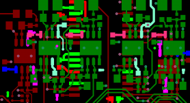
I have attached the layout for a different board, below. I'd like some feedback/criticism.
For this board I tried to use a ground plane, since some people stress this for best grounding performance. Its a 2-layer board with one layer mostly ground plane. I did connect any and all ground/common connections in the circuit into the ground plane. The layout is attached. Sorry about the colors again; red = top layer, blue = bottom. It's only a 2 layer board.
I was not at all satisfied with the result. I found that noise pickup was problematic for this layout. Why might that be the case?
.
Attachments
Last edited:
I have attached the layout for a different board, below. I'd like some feedback/criticism. I was not at all satisfied with the result.
I found that noise pickup was problematic for this layout. Why might that be the case?
.
There are lots of cuts in the ground plane. I would have moved more of the red traces to the other side.
What kind of noise problem? Can you post the schematic? Was the pcb mounted with metal hardware,
possibly shorting the ground plane to the chassis?
Last edited:
In todays RF rich environment you do have to worry about high frequency.
I agree put the traces on the other side and flood ground between pins.
Some of the VTLs could rotate 90 deg then you can get a trace between them pins allowing you to remove more red traces.
Again having a schematic to reference to makes life easier.
From first impression there is a lot of tracks spread out (forming unintentional dipole structures) often trying to do a universal design can add to many compromises.
As this is 2.54mm based design....
Sorry we have cousins from across the pond🙂
As this is a 100 thou based design, use 12 thou for tracks and 12 thou for gap and you can easily get a track (or a ground pour) between device pins, this will allow you to minimise trace lengths and get a much better ground pour, without the slots.
When ever I m doing any analogue layout I try to get all the signals single sided where possible, playing about with placement is critical here....
A similar thing here only surface mount....
Attachments
In todays RF rich environment you do have to worry about high frequency. When ever I m doing any analogue layout I try to get all the signals single sided where possible, playing about with placement is critical here.
That's right. My early days of making single sided pcbs really paid off later when going to double sided boards.
You get much better ground planes when you have most of the traces on the other side, but that's hard without
the prior experience of doing single sided by necessity.
Here's another question I have about the ground plane concept: since I am using a 2-sided board, the signal and ground sides are separated by the PCB epoxy board itself. Is that OK? Does a ground plane need to be the layer "right next to" the signal layer it is serving? For instance, would a board with a "back" layer, then the epoxy board, then ground plane and then signal plane be better?
Here's another question I have about the ground plane concept: since I am using a 2-sided board, the signal and ground sides are separated by the PCB epoxy board itself. Is that OK? Does a ground plane need to be the layer "right next to" the signal layer it is serving? For instance, would a board with a "back" layer, then the epoxy board, then ground plane and then signal plane be better?
Yes, this is how multilayer pcbs are done, it's a matter of via path lengths and loop areas. The closer together the planes are, the better.
Even the pcb material can affect the performance. But, the planes must be as solid, cut free, as possible.
Yes.Have you read Tomchr chipamp Thread? trace routing turned out to be critical to trying to match the discrete wiring prototype. In the end he IMPROVED the PCB version to better than National specifications, which came as a surprise to me and him.
I think this is the thread Andrew is referring to:
http://www.diyaudio.com/forums/chip-amps/252436-lm3886-pcb-vs-point-point-data.html
Proper management of the signal routing, finding a good ground reference (hint: use the ground at the voltage you care the most about), and minimizing the inductance of the routes were instrumental in achieving good performance. For precision circuits, the layout is the circuit. The schematic is just along for the ride... 🙂
~Tom
Regarding the many devices don't have a ground pin, I read what you said and asked the question, I think you will find there are very few that don't have a ground pin, if any, I cant recall seeing any.
Easy to think of quite a few - opamps and parts that behave like opamps e.g. chipamps. Opamps and chipamps make up a huge proportion of audio-related ICs.
Passing on from the issue of decoupling...
Here's a diagram of the currents in a somewhat idealised dual-rail DC-coupled, non-inverting amplifier.
Quiescent current flows all the way round the loop, output current flows alternately from the positive rail thru the device, out of the output, thru the load and returns to the junction of the supplies, or flows into the output being drawn thru the load from the junction of the supplies, thru the device and hence to the negative rail.
We can see that with 0V input, pins 3, 2 and 1 are all at 0V.
If we apply an input of 2V (neglecting source impedance), the current in R3 is 40 microamps, this flows back to the source. We're saying the amp input has infinite impedance.
The amplifier drives the output to 12V, forcing pin 2 to match pin 1 at 2V. The current through R2 is 20mA
The current through R4 is 1.5A.
Now you get to see the significance of the junction between the two voltage sources as pointed out by tomchr. When we want to return 1.5A to this point, we can see that it needs to be electrically robust if it is not to be disturbed, why we might even need to think about its inductance, since we can expect the current to change fairly fast, and why the return from the load connects directly there not via the input and feedback grounds. This point is frequently the junction between the nearest bulk supply capacitors and the device.
Representative magnitudes of the return currents elsewhere are also shown.
Here's a diagram of the currents in a somewhat idealised dual-rail DC-coupled, non-inverting amplifier.
An externally hosted image should be here but it was not working when we last tested it.
Quiescent current flows all the way round the loop, output current flows alternately from the positive rail thru the device, out of the output, thru the load and returns to the junction of the supplies, or flows into the output being drawn thru the load from the junction of the supplies, thru the device and hence to the negative rail.
We can see that with 0V input, pins 3, 2 and 1 are all at 0V.
If we apply an input of 2V (neglecting source impedance), the current in R3 is 40 microamps, this flows back to the source. We're saying the amp input has infinite impedance.
The amplifier drives the output to 12V, forcing pin 2 to match pin 1 at 2V. The current through R2 is 20mA
The current through R4 is 1.5A.
Now you get to see the significance of the junction between the two voltage sources as pointed out by tomchr. When we want to return 1.5A to this point, we can see that it needs to be electrically robust if it is not to be disturbed, why we might even need to think about its inductance, since we can expect the current to change fairly fast, and why the return from the load connects directly there not via the input and feedback grounds. This point is frequently the junction between the nearest bulk supply capacitors and the device.
Representative magnitudes of the return currents elsewhere are also shown.
Last edited:
- Status
- Not open for further replies.
- Home
- Source & Line
- Analog Line Level
- understanding source+return current flow on PCBs