hello forum!
the following circuit was thrown together just so i could play with LTspice. it may not make sense in many regards, but i'm now after techniques in lowering THD in cases similar to this.
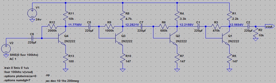
when i simulated in the following two ways, i got these THD numbers. in both cases, signal is amplified from 5.0uV to about 1.1V.
1khz
50ms
THD=0.022516%
100khz
5ms
THD=2.432877%
as merely a circuit exploration, what are some of the well known, time proven, and rather effective techniques around that i should try here, in order to lower the THD, expecially in the 100khz case?
thanks a lot for helping!
the following circuit was thrown together just so i could play with LTspice. it may not make sense in many regards, but i'm now after techniques in lowering THD in cases similar to this.
when i simulated in the following two ways, i got these THD numbers. in both cases, signal is amplified from 5.0uV to about 1.1V.
1khz
50ms
THD=0.022516%
100khz
5ms
THD=2.432877%
as merely a circuit exploration, what are some of the well known, time proven, and rather effective techniques around that i should try here, in order to lower the THD, expecially in the 100khz case?
thanks a lot for helping!
Attachments
Last edited:
Member
Joined 2009
Paid Member
This is DIY Audio, what I think you need is DIY Radio. At 100kHz most of us are not paying too much attention 🙂
At that frequency it's hard to implement a popular solution for THD reduction, namely global negative feedback, because you have 4 amplifier stages and the phase shift will likely make it unstable.
Try more local feedback from collector-to-base ?
Try using JFETs ?
At that frequency it's hard to implement a popular solution for THD reduction, namely global negative feedback, because you have 4 amplifier stages and the phase shift will likely make it unstable.
Try more local feedback from collector-to-base ?
Try using JFETs ?
...
At that frequency it's hard to implement a popular solution for THD reduction, namely global negative feedback, because you have 4 amplifier stages and the phase shift will likely make it unstable.
could you please explain the kind of phase shift 4 stages will produce which will make the circuit unstable as a result? i have no idea how phase shift works. tks!
Global negative feedback means connecting or mixing the output back into the input in a way that it subtracts from the input. This throws away some of the gain in exchange for better accuracy or less distortion.
In this case, since there are an even number of inverting common emitter stages, you'd probably have to jam it into the emitter of the first stage through a resistor, since simply mixing it into the base would be positive feedback rather than negative.
The phase shift is not constant with frequency. To understand how it can cause oscillation, think of it as a time delay. For a sine wave whose period is twice the delay, a connection that was negative feedback for sufficiently slow signals becomes positive feedback. If the frequency response of the amplifier is such that it still has some gain at that frequency, the system will oscillate when the feedback loop is closed.
There's nothing special about four stages; just that each stage adds more delay and more gain, thus raising the chance that you still have gain at the frequency where the feedback becomes positive.
Also, there are well-studied techniques for stabilizing ( preventing oscillation with ) nfb in amplifiers with two voltage gain stages that don't apply to or are much harder to use for three or more stages.
Nevertheless, you could try connecting a resistor from the output to the emitter of the first stage to see what happens.... then maybe even increasing the collector resistance of a stage to make up for the gain loss from the nfb ...
Last edited:
Here are a couple interestingly good papers about nested feedback/feedforward loops, linearization techniques.
I bet with some THAT matched arrays or devices similar for the error transistors, one could make just about any transistor quite linear in operation.🙂
I bet with some THAT matched arrays or devices similar for the error transistors, one could make just about any transistor quite linear in operation.🙂
Attachments
Last edited:
Fewer stages with higher gain in each stage, with global feedback applied, would likely reduce distortion and definitely have less phase shift too.
Your circuit is so 1965 anyway. It's instructive, but not practical.
Your circuit is so 1965 anyway. It's instructive, but not practical.
To start with, I think the high value of THD at 100 kHz is just simulator error. It looks like you've got max timestep set to 1uS. That's fine for testing at 1kHz, but for 100kHz it should be much lower - maybe 0.01uS.... to lower the THD, expecially in the 100khz case?
You can't put global negative feedback around such a circuit, as others have explained. You could increase the local feedback in the final stage, which is where most of the distortion will be produced. Increase the emitter resistor. Reduce the base and collector resistors, so the stage runs with more current.
What I suggest you do is take the final stage on its own. Feed in a signal. Adjust the resistors, and so the local feedback and the stage current. See how the gain and distortion varies. Learn how to calculate what the simulation shows you, at least approximately. Then you will be in a good position to start designing.
What I suggest you do is take the final stage on its own. Feed in a signal. Adjust the resistors, and so the local feedback and the stage current. See how the gain and distortion varies. Learn how to calculate what the simulation shows you, at least approximately. Then you will be in a good position to start designing.
hey alright guys, a whole bunch of very useful and helpful replies, i'm certainly learning! thanks a whole lot for talking to me about DIYradio!🙂
i'll put these ideas on my todo list, and give them a try in due time!
i'll put these ideas on my todo list, and give them a try in due time!
To start with, I think the high value of THD at 100 kHz is just simulator error. It looks like you've got max timestep set to 1uS. That's fine for testing at 1kHz, but for 100kHz it should be much lower - maybe 0.01uS.
very sharp eyes godfrey, and thank you for pointing that out!
i tried 0.01us, but it ran so slow, with the running time unchanged, at 5ms, after about 15 minutes, it's still at 2.4% done. so i changed the running time to 100us, and got something like this.
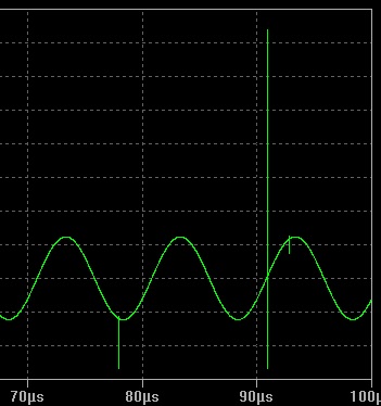
i don't know what those vertical lines mean, but the THD is down to 0.063673% from 2.432877%, much better.
i also tried .tran 0 5ms 0 0.1us, it ran pretty fast, and the THD is down to 0.080357%.
so choosing the right simulation setting certainly made a huge difference. how do i judge what a good simulation setting, max timestep and run time etc., is for a simulation? any rule of thumb here?
Attachments
Last edited:
...
There's nothing special about four stages; just that each stage adds more delay and more gain, thus raising the chance that you still have gain at the frequency where the feedback becomes positive.
i'm not sticking to any particular number of stages, because i don't have an actual application for it, it so happened by chane, so i let it be. i'd like to put the emphasis on techniques of lowering THD now. with 4 stages, the question of stability also comes into focus, that's great, i can learn about that as well. 🙂
Nevertheless, you could try connecting a resistor from the output to the emitter of the first stage to see what happens.... then maybe even increasing the collector resistance of a stage to make up for the gain loss from the nfb ...
thank you for explaining all that to me mirlo! now i know what bigun means by phase shifting.
i added a NFB like this, and adjusted the values of the NFB resistor as well as the emitter resistors so that the output is about 1.1V.
with .tran 0 5ms 0 0.1us, the THD is 0.100258%.
this THD number is not as low as without global NFB, and each stage all had less gains, that number is 0.080357%.
am i doing this wrong? or should i conclude having less gain with each stage and no global NFB is the way to go? or instead of trial and error, i should resort to math for a direction?
Attachments
Last edited:
Here are a couple interestingly good papers about nested feedback/feedforward loops, linearization techniques.
I bet with some THAT matched arrays or devices similar for the error transistors, one could make just about any transistor quite linear in operation.🙂
thank you for the good pointers CBS240, my troubles started out as fun as well!🙂
reading... doing homework now...
Fewer stages with higher gain in each stage, with global feedback applied, would likely reduce distortion and definitely have less phase shift too.
Your circuit is so 1965 anyway. It's instructive, but not practical.
thank you for the help Fast Eddie!
does 65 mean BJT's don't have as high a gain as they are now, and more stages were necessary back then?
i'll give less number of stages and each stage having more gains a try.
You can't put global negative feedback around such a circuit, as others have explained. You could increase the local feedback in the final stage, which is where most of the distortion will be produced. Increase the emitter resistor. Reduce the base and collector resistors, so the stage runs with more current.
What I suggest you do is take the final stage on its own. Feed in a signal. Adjust the resistors, and so the local feedback and the stage current. See how the gain and distortion varies. Learn how to calculate what the simulation shows you, at least approximately. Then you will be in a good position to start designing.
thank you for the suggestion DF96!
actually i did each stage separately before i put them together. all had very low THD individually, the last stage for example had THD=0.000360%, 1khz, 5ms run time, max timestep 1us. but when i put them all together, things changed a lot, i got 0.051267% as a whole. thus the question. of course i didn't give most of the gain to the last stage, i kind of spread the gain out evenly among all stages. i'll try concentrate most gain on the last stage and try to deal with it mostly at that stage, and see what.
Last edited:
thank you for the help Fast Eddie!
does 65 mean BJT's don't have as high a gain as they are now, and more stages were necessary back then?
No. The design is for all practical purposes obsolete. It is instructive, though.
Circuits like this were actually used in early transistor equipment. They are similar to tube circuit configurations from way back. Even the better tube circuits from the 50s and 60s typically had better topology than this circuit; at least equipment marketed as "high fidelity."
Its advantages are that it is easy to troubleshoot and did not suffer from instability problems.
I would take your simulations with a grain of salt too; although they can certainly help to point you in the right direction.
i'll try concentrate most gain on the last stage
You want your voltage gain up front. Configure the last stage for current gain.
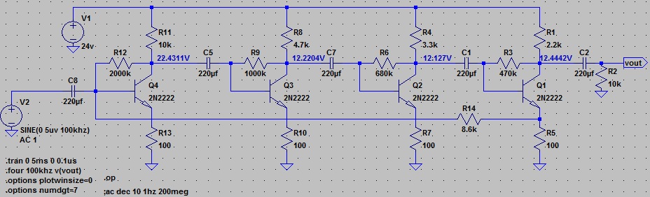
The way you have the feedback connected may be affecting the bias point a lot by pulling down the base of q4. It also doesn't give much nfb because the driving impedance ( the ideal signal source followed by 220uF ) is such a low impedance compared to the 8k feedback resistor. In fact, its action is more feedforward, adding the input signal into the final stage through emitter of q1 acting as a common base stage rather than back from output to q4's base input. Instead, perhaps try connecting the feedback resistor from the output after C2 to the junction of R13 and q4's emitter.
Last edited:
Last edited:
Do an image search on two transistor amplifiers. A lot of old RIAA preamps got pretty good gain and pretty low THD out of two transistors, just leave out the eq network. In hindsight they weren't terribly good, but it's a great place to start. Also search high gain FET cascode. In their ancient app notes, National had a couple very simple two device circuits that worked well.
The way you have the feedback connected may be affecting the bias point a lot by pulling down the base of q4. It also doesn't give much nfb because the driving impedance ( the ideal signal source followed by 220uF ) is such a low impedance compared to the 8k feedback resistor. In fact, its action is more feedforward, adding the input signal into the final stage through emitter of q1 acting as a common base stage rather than back from output to q4's base input. Instead, perhaps try connecting the feedback resistor from the output after C2 to the junction of R13 and q4's emitter.
great help mirlo!
i'm learning, picking up things, hopefully i'd know more, overtime, on what to consider, what to look for, how to analyse the circuit, recognizing the operating state a circuit is in, and acquiring the necessary techniques in dealing with issues, etc.. i'm learning about all that from your replies, thank you!
i did what you recommended, and... i got oscillation🙁. here is the fft of this circuit in oscillation.
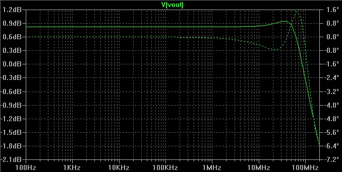
i don't know how to read this diagram,
how do i tell whether there is an unstable phase shift or not?
what is considered as a stable phase shift state?
and what can be done to stop the oscillation?
actually it is good that it's oscillating, i can learn about it now, gain some understanding about it, and hopefully acquire the ability of dealing with it in possible future situations.
i tried taking the last stage out, and it worked, no oscillation. i'm pursuing this 4-stage thing just for the sake of learning. if there are better directions in exploring all these circuit issues, topology, distortion, noise, frequency response, stability, etc., than pursuing this arbitrary 4-stage thing, please let me know. i don't have to hold onto this weird 4-stage thing, but i do want to hold onto the exploration of the above mentioned circuit issues.
thank you for your time!
Attachments
a very good guide, already translated as well!
i'm using his techniques now, especially for accurate max steptime, runtime, and resolution.
great, i'm learning, becoming more capable than before, little by little!
thank you very much mirlo!
Last edited:
- Status
- Not open for further replies.
- Home
- Amplifiers
- Solid State
- how to lower THD in small signal BJT amps?