I have been using a LM3875 Gainclone for a few months now and I am very happy with it.
I am running it at ~26V (18VAC secondaries) for a conservative power output with both my 93db 8ohm and 92db 4ohm speaker sets.
I am following the usual schematic more or less, with additional 10000uF caps for extra bass.

What bothers me is the lowish input impedance that is forcing me to use big and lower quality coupling caps with my DCB1 (on top of being a harder load), and the fact that I have way more gain than I need in my room (trying to also perhaps reduce the effect of the pot in my dcb1)
What I am considering, is to actually increase the input impedance to 100K and reduce the gain to around 24dB
With R2 at 100K (no pot, driven directly by dcb1), R4 is also 100K to minimize dc offset, and for ~24dB gain, R3 is ~4.3K
From what I can tell from the datasheet, operation should be well below the spike trigger point
This would allow the use of a very nice quality 0,47uF coupling cap (teflon or something). But I am also considering to remove the coupling cap after DCB1, and instead use a 10uF feedback shunt to zero DC gain where the effect of the cap will be compensated by the fast feedback operation.
Finally, I am thinking of going further to 200K input impedance (like my previous electrocompaniet amps) and/or try to replace the "spiked" 3875 with its small brother 1875, but I would probably have to reduce the voltage a bit to keep it in safe operating regions.
I have tried to read a lot and study the datasheets, but I am still pretty novice in chipamps and opamp operation theory, so any feedback would be greatly appreciated.
I am running it at ~26V (18VAC secondaries) for a conservative power output with both my 93db 8ohm and 92db 4ohm speaker sets.
I am following the usual schematic more or less, with additional 10000uF caps for extra bass.
What bothers me is the lowish input impedance that is forcing me to use big and lower quality coupling caps with my DCB1 (on top of being a harder load), and the fact that I have way more gain than I need in my room (trying to also perhaps reduce the effect of the pot in my dcb1)
What I am considering, is to actually increase the input impedance to 100K and reduce the gain to around 24dB
With R2 at 100K (no pot, driven directly by dcb1), R4 is also 100K to minimize dc offset, and for ~24dB gain, R3 is ~4.3K
From what I can tell from the datasheet, operation should be well below the spike trigger point
This would allow the use of a very nice quality 0,47uF coupling cap (teflon or something). But I am also considering to remove the coupling cap after DCB1, and instead use a 10uF feedback shunt to zero DC gain where the effect of the cap will be compensated by the fast feedback operation.
Finally, I am thinking of going further to 200K input impedance (like my previous electrocompaniet amps) and/or try to replace the "spiked" 3875 with its small brother 1875, but I would probably have to reduce the voltage a bit to keep it in safe operating regions.
I have tried to read a lot and study the datasheets, but I am still pretty novice in chipamps and opamp operation theory, so any feedback would be greatly appreciated.
Attachments
Last edited:
.
<< What I am considering, is to actually increase the input impedance to 100K >>
Nothing to it. You're talking about a buffer, which is long-mature technology.
The whole purpose of a buffer is to separate an audio source from a following circuit. In essence source sees no load at all.
Connected with 100% feedback as shown, most op amps become a buffer. The characteristics of a buffer are unity gain, extremely high input impedance (in the tens of megs or higher), and extremely low output impedance (single digit). Distortion is negligible, in the three-decimal range.
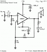
I've posted a circuit below. It looks a bit lopsided because it's actually an el quickO edit down from a larger circuit, edited down to what I think are your needs.
The input circuit is a rip from Douglas Self. R1 and C1 shunt noise to ground. C2 and R2 are, of course, a high-pass filter.
R3 is a just-in-case resistor to prevent oscillation. It theoretically does nothing, since there's theoretically no current flow.
R4 reduces volume as you wished. It forms a voltage divider with your existing 10k input pot, and simply dissipates half the input signal. True this is wasting half the input, but it's no different from keeping the volume turned down. The 10k value is a guesstimate on my part. Maybe 5k?
The circuit is shown as direct coupled (no output capacitor) because output errors are expected to be insignificant. Another guesstimate.
With a 100k Zin you're well into Johnson noise territory, and noise can become a problem in general. You might want to consider reducing R2 to 56k or thereabouts. You could leave C2 at 0.33uF, or adjust it as wished.
Component specs are simply what's commonly available on eBay. Of course you can go higher and tighter if you like. Other ICs could work (no guarantees which will or won't), but I doubt there'd be any real improvement.
Hope this might be of some interest.
.
<< What I am considering, is to actually increase the input impedance to 100K >>
Nothing to it. You're talking about a buffer, which is long-mature technology.
The whole purpose of a buffer is to separate an audio source from a following circuit. In essence source sees no load at all.
Connected with 100% feedback as shown, most op amps become a buffer. The characteristics of a buffer are unity gain, extremely high input impedance (in the tens of megs or higher), and extremely low output impedance (single digit). Distortion is negligible, in the three-decimal range.
I've posted a circuit below. It looks a bit lopsided because it's actually an el quickO edit down from a larger circuit, edited down to what I think are your needs.
The input circuit is a rip from Douglas Self. R1 and C1 shunt noise to ground. C2 and R2 are, of course, a high-pass filter.
R3 is a just-in-case resistor to prevent oscillation. It theoretically does nothing, since there's theoretically no current flow.
R4 reduces volume as you wished. It forms a voltage divider with your existing 10k input pot, and simply dissipates half the input signal. True this is wasting half the input, but it's no different from keeping the volume turned down. The 10k value is a guesstimate on my part. Maybe 5k?
The circuit is shown as direct coupled (no output capacitor) because output errors are expected to be insignificant. Another guesstimate.
With a 100k Zin you're well into Johnson noise territory, and noise can become a problem in general. You might want to consider reducing R2 to 56k or thereabouts. You could leave C2 at 0.33uF, or adjust it as wished.
Component specs are simply what's commonly available on eBay. Of course you can go higher and tighter if you like. Other ICs could work (no guarantees which will or won't), but I doubt there'd be any real improvement.
Hope this might be of some interest.
.
Attachments

Thanks a lot for your effort
About further cutting the input signal, if we already cut it with a pot, there is no need to cut it again with an additional divider. I wanted to reduce the gain so that a smaller part of the pot is in series with the signal.
About the noise, I have read a bit about it with bigger resistor values, but I have no opinion on when it happens. I will consider your suggestion for ~50K which should make a nice difference anyway.
I am not talking about an additional buffer (I already have a dcb1). I am talking about adjusting the gainclone for bigger input impedance, so that it is an easier load for everything (including buffers) and allow for a smaller coupling cap.Nothing to it. You're talking about a buffer, which is long-mature technology.
The whole purpose of a buffer is to separate an audio source from a following circuit. In essence source sees no load at all.
About further cutting the input signal, if we already cut it with a pot, there is no need to cut it again with an additional divider. I wanted to reduce the gain so that a smaller part of the pot is in series with the signal.
About the noise, I have read a bit about it with bigger resistor values, but I have no opinion on when it happens. I will consider your suggestion for ~50K which should make a nice difference anyway.
.
<< I am not talking about an additional buffer (I already have a dcb1). >>
I have no idea what a dcb1 is, but hey, noprob.
.
<< I am not talking about an additional buffer (I already have a dcb1). >>
I have no idea what a dcb1 is, but hey, noprob.
.
you can put a buffer after the volume pot, going directly to the chip amp input
you could find a op amp with a decent Vos spec so that it can be DC coupled to the chip amp +input
or even better, rewire the chip amp for inverting gain
you need to use compensation tricks to safely reduce the feedback determined gain - these chip amps all have high minimum gain settings for stable operation
inverting operation makes the noise gain compensation easier too if still need to reduce gain
From what I remember 20db is the minimum recommended gain for that chip implementation, so 24dB should be pretty safe from a stability point of view.
About the buffer, again I am using a salas DCB1, but I am using it AC coupled for extra safety because it is really hotroded
About the buffer, again I am using a salas DCB1, but I am using it AC coupled for extra safety because it is really hotroded
Lets not further analyze here if Nelson Pass or Salas is a guru in quotation marks with cute named projects.
Lets just say that my first stage buffer works very well and I do not want to (not to mention cannot) build and optimize a new opamp stage to replace it.
Lets just say I just want to optimize a bit my final amplifying stage to make it an easier load and decrease its gain, choosing values very close to ones suggested on the datasheet itself.
Any comments on the changes I proposed ?
Here is an updated schematic to make things clearer on what I want to work with.

So far I am keeping the warning about noise from the 100K resistors.
Lets just say that my first stage buffer works very well and I do not want to (not to mention cannot) build and optimize a new opamp stage to replace it.
Lets just say I just want to optimize a bit my final amplifying stage to make it an easier load and decrease its gain, choosing values very close to ones suggested on the datasheet itself.
Any comments on the changes I proposed ?
Here is an updated schematic to make things clearer on what I want to work with.
So far I am keeping the warning about noise from the 100K resistors.
Attachments

Non of these are ideal solutions.
You now show a 100k input impedance and a 4.3k feedback return. That is probably going to create a significant DC offset unless you now AC couple the 4.3k to ground. Keeping feedback and input resistors the same only works for DC offset when the feedback return is AC coupled.
Noise from the 100k input resistor isn't such a problem because it is shunted by the preamp output impedance.
There is no easy to achieve what you want without a redesign I'm afraid.
Non of these are ideal solutions.
You now show a 100k input impedance and a 4.3k feedback return. That is probably going to create a significant DC offset unless you now AC couple the 4.3k to ground. Keeping feedback and input resistors the same only works for DC offset when the feedback return is AC coupled.
Noise from the 100k input resistor isn't such a problem because it is shunted by the preamp output impedance.
There is no easy to achieve what you want without a redesign I'm afraid.
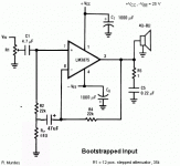
I was thinking to add the shunt capacitor. 10uF in series between R3 and earth
That would solve the DC offset issue as long as your input is AC coupled at the point marked Vin on your circuit.
Will this work?
edit: this is to solve the low input impedance issue.
I'm sure OP knows how to lower gain.
edit: this is to solve the low input impedance issue.
I'm sure OP knows how to lower gain.
Attachments
Last edited:
I see what you are trying to do... yes in theory that would work and give a very high input impedance. You would need to try it for real and perform all the usual tests... stability, squarewave response etc... but yes, a bootstrapped input is a workable solution.
.
Well, since you ask.
I don't know anything about the buffer you're using, but a buffer by its nature has (or should have) single-digit output impedance. This makes the input impedance of the following amp a non-issue, since all op amps have input impedances in the kilohm range at least.
With the buffer's high Zin, and low Zout, it seems you've already accomplished your goal, so changing Rin to something besides 10k seems to be meaningless.
Referring to the TI schematic, RB (1k in series with pin 7) has two (maybe 3) functions. First, under some conditions the op amp can go into self-destructive oscillation, but RB prevents this. Second, under some conditions the op amp can respond to spikes in the input signal and go into severe distortion. Again RB prevents this.
Possible third, it looks like RB is also a compensation resistor, approximately equalizing the impedances seen by the inverting and non-inverting inputs.
Under normal conditions RB has no significant effect on the input signal, I personally can see no reason for omitting it.
Again referring to the TI schematic, the function of Ci is to restrict DC gain to unity. This prevents the op amp from amplifying DC input/bias/offset voltages. Removing it loses this protection.
Still the TI schematic, the feedback network, the general rule with op amps is to keep resistance values as low as possible. I can't see any advantage to increasing the value of Ri, and therefore having to increase the value of Rf.
Lookee, I'm sorry to sound like the all-wise, or some kind of smarty mouth or something, but I just don't see how anything is gained.
On the other hand, if you just want to mess around and see what happens, well sure, why not. That's pretty much what we do around here.
.
Last edited:
I see your points and again thanks for you time.
They are pretty much the arguments against the simplistic schematics of gainclones.
About my buffer, it is actually implemented as a preamplifier in a separate case, so it uses 220R at the output to prevent instabilities by driving the cable capacitance and care for different final amplifying stages. Minimizing this impedance is my other goal.
I plan to get a proper signal generator at some point to be able to check everything with a proper square and reduce the output resistor to the minimum stable value.
- Status
- Not open for further replies.
- Home
- Amplifiers
- Chip Amps
- Lower gain, higher input impedance gainclone